On the bottom of the box I placed a piece of FR4 fiberglass PCB material (I etched completely both copper layers using a mixture of Hydrogen Peroxide and Hydrochloric (Muriatic) Acid (1:2))Wednesday, November 25, 2009
N2PK VNA - RF-IV Sensor
On the bottom of the box I placed a piece of FR4 fiberglass PCB material (I etched completely both copper layers using a mixture of Hydrogen Peroxide and Hydrochloric (Muriatic) Acid (1:2))Wednesday, November 4, 2009
N2PK VNA - Accessory Connector
The Accessory Connector must be at least 6 pins if an S-parameter setup will be connected. I am not planing to build one at this time and I need connector with only 3-4 pins for the power and control signal to the RF-IV sensor and possibly a transverters. Most people are using the Mini-DIN connectors (like the ones used for the PS/2 keyboard or mouse) but I am not really fond of these connectors - this type connector does not provide very secure connection and can be easily pulled apart.
The connector I ended up using is the HR10 type (Hirose Electric) Digikey P/N HR1568-ND (female, panel mount) and HR1558-ND (male, plug). This connector is superior to the Mini-DIN. It is available in 4 pin and 6 pin configurations, it is small and it has a very nice locking mechanism.
Not cheap by any means - a pair (male-female) will set you back almost $30 but it is very high-quality product (nice looking too).
Update Jan 2012: I am working on my S-parameter test set and I replaced the 4 pin connectors with the 6 pin version. I have 3 male and 1 female 4 pin HR10 connectors in excess of my needs. Price is $10 per connector + postage (~25% off Digi-key price). All connectors are used (were installed) but in pristine condition.
Tuesday, October 27, 2009
N2PK VNA - USB to Parallel interface
For my project I used a PCB from WB6DHW. His interface is a nearly identical clone (electrically) of the G8KBB interface. To be honest, I am less than impressed (other words, which I'll save come to my mind ) with the PCB layout done by WB6DHW - it looked like somebody was learning how to design a PCB and used this project as a practice board. I was almost ready to design my own board (G8KBB's board is excellent but his PCBs are not readily available). Don't mean to bash WB6DHW - just expressing an opinion. At the end of the day tho, I decided to close my eyes and got the bare board from WB6DHW because of its low price - fabricating my own board was going to cost a lot more and wasn't worth the effort/money just for a single piece. All components are from DigiKey, including the Cypress chip and the Hammond die-cast aluminum enclosure housing the interface.
Wednesday, October 21, 2009
N2PK VNA - RF-IV sensor PCB
The PCB is very simple and easy to work with. A thing to note is the slightly awkward placement of the RF connectors - it is needed to achieve certain level of port-to-port isolation. There are two transformers, one (on the left) takes the Current sample, the other (on the right) the Voltage sample - this part of the circuit is almost the same as in Larry's N8LP coupler for the LP-100. The DUT is connected to the RF DDS of the VNA thru the current transformer. The RF switches (Peregrine PE4220 ) are controlled by the software and switch the signal path of the samples to the RF DET input of the VNA. While the VNA takes a sample of the current (I), the voltage (V) transformer is terminated with 50 ohm load and vice versa. There is an on-board 3.3V voltage regulator supplying power to the RF IC switches. Only one detector is used in the VNA in this configuration which improves the stability and accuracy of the measurements as both -the I and the V samples are measured by the same detector alternatively at a high frequency. The control signal to switch between the samples is generated by the software and in this case is just looped thru the VNA.
Winding and installing the transformers is a bit tricky because of their construction and small size. One of the winding is done with very fine (AWG #36) wire. In addition, the current transformer (shown on the picture) has a grounded electrostatic shield between the primary and the secondary. Both transformers are attached to the board with tin-plated brass strips bent into U-shape. The strips provide RF screening and stress-relief at the same time.Tuesday, October 20, 2009
VNA plots of my SteppIR BigIR
All plots were generated with the myVNA software. Calibration of the VNA was performed at the far end of the 100ft feedline to tune-out the transformation effects of the transmission line.
The scan was done while the antenna was tuned for minimum SWR on the 20m band.
The graphs can be seen here
Thursday, October 8, 2009
N2PK VNA - It is a "Lab in a Box"!
(btw. Here is a link to a very informative document about the VNA basics by Agilent)
As one can see - attenuation is only 63 dB at 54 Mhz with maximum attenuation of 66.5 dB at 57 MHz - that is pretty far from the claimed "80 dB". This screen-grab shows the true beauty of the Dual Detector setup - for example being able to plot the VSWR curve in reflection mode at the same time as the attenuation curve in transmission mode.
Its not only a VNA - it is a handy signal generator - myVNA software allows you to use it as adjustable signal generator. This picture shows a rough frequency measurement (my scope has current calibration), 14 Mhz - same as the value set in the software. (the oscilloscope of course can't measure with such great resolution as what the software allows you to adjust but gives an idea about the clean sine wavefrom generated by the DDS).
Among other things - there is a vector volt-meter available in myVNA. This image shows the result of -10 dBm output measured thru a variable precision attenuator (set to 8dB) at 6 MHz : -18.0026 dBm. I'd say pretty accurate! The vector voltmeter can use both ADC at the same time for measurements and display the phase difference as well.
Plot of the Return Loss of my LMR-600 coaxial feedline going to the SteppIR vertical. The length of the cable is exactly 100 ft (+/- 1 ft). The graph shows a Return Loss of approx. 1.2 dB @ 50 MHz. The actual loss is one half of the measured RL (just one way) or 0.6 dB @ 50 MHz. Times Microwave specs for LMR-600 are listed as 0.5 dB @ 50 MHz per 100 ft. A 0.1 dB difference is insignificant (I have connectors on both ends and I used a BNC-to-N adapter for the measurement). The cable is under ground in a PVC conduit (hopefully watertight) but I can keep an eye on the losses with the VNA.
Here is another interesting plot. This graph shows the Return Loss of my entire station - from the transceiver antenna connector to the antenna feed-point connector 100 ft away. The signal path includes a RF patch bay, 2 coaxial switches, 2 directional couplers, gas-discharge lightning arrester, ACOM 1000 amplifier, common-mode choke, well over 100 ft of coaxial cable (in transmission line and jumpers) as well as a large amount of UHF and N connectors.Detailed RF signal path in the AE1S station can be seen in an old post - here
The loss is approx 1.9 dB on 6 meters (again RL/2) and between 0.3 dB and 1.25 dB on the HF bands. Not bad at all, keeping in mind what is on the signal's path!
The two distinctive "peaks" on the graph are caused by the ACOM 1000 amplifier. These peaks represent the self-resonance of a built-in choke in the amp. The good news is that they are located outside of the amateur bands.
... and I am just scratching the surface of this great instrument!
Wednesday, October 7, 2009
N2PK VNA Calibration Standards
Here are some notes on the calibration standards for the N2PK VNA. Initially, I've made my own Open-Short-Load-Thru kit. My VNA is equipped with BNC connectors, so I used "clamp type" male BNC connectors for large diameter coaxial cable (such as LMR400/RG-8) to house my calibration standards. I also wanted to have some reference calibration standard to compare against.
I was able to acquire (tnx to eBay) a precision commercial VNA calibration kit at very reasonable price. I did some comparison between my home-brewed calibration standards and the Maury Microwave VNA Kit (MMC) - good for VNA calibration DC to 18GHz.
I wanted all of my cal standards to use the same type of housing in order to easily maintain the same reference plane. Looking at the commercial standards - that's not case - the shells are different size but the reference plane inside must be the same.
As expected, the home-brewed Open and Short standards (which are fairly easy to fabricate), when compared to the expensive commercial standards seem to be pretty close. The Short standard must have low inductance and the Open - low capacitance. Looking at the MMC Short standard - it seems to be made out of one piece of metal for the center pin and the ground shell - the electrical short occurs at the far end of the center pin right at the back-face of the actual connector and the pin's length seems to be shorter than the normal N-connector center pin. The commercial MMC Open load has longer center pin attached to a dielectric disc in the back of the housing but maintains the same "reference plane".
The story is much different for the 50 Ohm Load standard. I made two different Load standards using different components (bulk-metal foil resistor and edge-trimmed precision thin film resistor - both rated for high frequency use and optimized for minimal self-reactance) and different construction techniques. Both Loads turned out to be not as good as the MMC Load (which I kind of expected) but the Load with the expensive bulk-metal foil resistor seems to be worse than the thin-film one. I suspect the difference is due to the construction and the much larger SMD component.
In addition, I tested the combination of a Male BNC-to-female SMA adapter + home-brewed SMA Load (housed in RA male SMA connector shell, /w edge-trimmed thin-film resistor) was much closer to the commercial MMC Load and actually quite acceptable.
I'll be trying yet different construction technique for the BNC Load standard. The main challenge with the BNC Loads is the installation of the SMD resistor. The center pin of the BNC is not captive, and it needs to be fixed somehow in order to remove any mechanical stress form the resistor. So far I have not used any glue or epoxy in my cal standard constructions, but I think it is about time to try it.
Here is the 50 Ohm LOAD standard using a Vishay FC series, high frequency precision (0.1%) 0603 SMD resistor - Digikey p/n FC0603-50BWCT. This size resistor is a perfect fit between the barrel and the center pin. The center pin of the connector is trimmed down, and the resistor is soldered in place.
The other two standards - OPEN and SHORT were very easy to make! One should be careful when soldering the SHORT standard not to melt the center insulator with excessive heat (I used a water bath during soldering). On the OPEN standard the center pin must be trimmed down to keep the reference plane the same across all 3 standards.
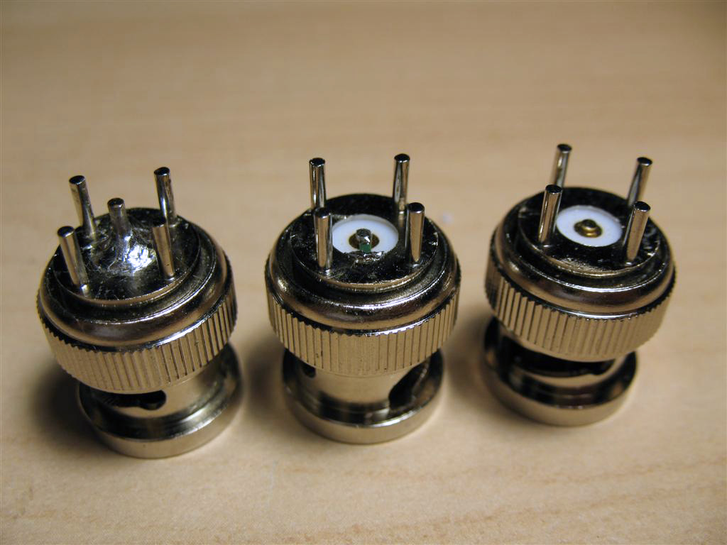
In order to create RF shielding, provide mechanical protection and facilitate easier handling, I prepared 3 short pieces (~1 cm length) - 2 made with brass tubing (Stock #137, K&S Engineering, 7/16" (11.1mm)) and one of same diameter plastic tube (used for the OPEN standard). I soldered each piece on the inside to the 4 ground pins of the SHORT and LOAD BNCs. Closed-cell foam was used create an endcap for each barrel. The LOAD standard was closed on the back with additional RF shield - tin-plated brass disc, soldered to the inside wall. The body of the OPEN standard was made with the plastic sleeve and glued to the 4 BNC pins - the reason for using plastic is to reduce stray capacitance, caused otherwise by a brass sleeve.
Tuesday, September 22, 2009
N2PK VNA - Some initial plots
Quick sweep (3 to 29 MHz) of my G5RV clearly shows the low SWR points. It also reminds me that I need to do some minor tuneup of the antenna. The red vertical cursor is at the CW portion of the 20m band - the other SWR dips are in agreement with what should one expect from the classic G5RV. A VNA makes the ultimate antenna analyzer! One extremely valuable feature is the ability to perform calibration at the end of the coax / antenna feed point thus removing the impedance transformation effect of the coax from the measurement! It is like having the VNA connected right at the antenna feed point. (A good overview of various antenna analyzers and designs (incl. N2PK) can be found here )N2PK - Final Assmebly
I am very satisfied with the results - a very precise, lab grade instrument in a professionally looking package - one can hardly tell that it is not a "commercial product".
The initial testing went just fine as expected. I spent a lot of time, making sure that everything is done right, inspecting every single solder joint and checking every component so I was not expecting any major problems. Everything worked the first time I plugged it in!
A note to myself: Next time I decide to build something with 7 bulkhead BNC connectors on the front panel - get a Greenlee D-hole punch. Shaping that many D-shaped holes with a regular drill and a file was tedious work. My method of using Clear ink-jet mailing labels and 3M laminating sheets resulted in a superb quality panel finish. The colors on the panels are just a hint how much fun is to use the instrument :-)
The last touch before closing the unit was to attach a spare fuse to the PS board :) (hopefully I won't need it)
It is a pretty tight install - once everything is in place and connected, there is not much space wasted in the Hammond enclosure.
2010 Update: This picture shows the final version, using semi-rigid coax (RG-405) for Detector inputs and RF DDS out. The coax is in black heat-shrink tubing - just did not like the idea of exposed conductors crossing above the VNA PCB. The control/power cables were re-organized too and an accessory connector was installed.
The Hammond enclosure comes with two elegant bezels for the front and rear panels. When the bezels are installed, they stand between the enclosure and the panels. Under "normal" circumstances (DC/low frequency applications) this is OK. Since these bezels are plastic, the face-plates are electrically connected to the enclosure only with the 4 corner screws. In the RF world things are a little different. The electrical gap which occurs because of the plastic trim can cause signal leakage to and from the VNA. It degrades the overall RF shielding of the aluminum enclosure and affects the impedance-to-ground of the front panel connectors. I solved this issue with 6mm strips of self-adhesive copper foil - I wraped the 3 surfaces of the inside plastic edge with copper foil, covering all 4 sides of the bezel. When the plastic bezel is sandwiched between the panels and the enclosure, the copper foil serves as electrical bridge between the aluminum face-plates and the enclosure, while creating continuous RF shield on the inside.
This is the complete set - VNA, Reflection bridge and OSL calibration standards.Since the calibration standards determine the accuracy of the measurements, I paid extra attention while building them. For the 50 ohm load I used small (0603) thin-film resistor - optimized for high frequency use (up to 20GHz) (Digikey P/N FC0603-50BWCT-ND or FC0603-50BFCT-ND). The construction of the OPEN and SHORT standards was also done very carefully. I am planing to make 2 more sets of calibration loads - N-type, SMA and UHF loads. This way I can use adaptors BNC-to-"X" and calibrate after the adaptor or at the end of the jumper cables regardless of their type and without using more adaptors.
The last thing left to do is to organize everything in a Pelican 1450 protective case.
Hmm...now thinking about this RF-IV sensor ... it doesn't look like the build is really over :-))
Feb 2011 Update - My complete VNA kit fits nicely in a Pelican 1500. This case is water-tight, very durable and makes it convenient to store and transport the VNA with all of it's accessories.
N2PK VNA Main board RF shielding
I made the RF shield cans out of tin-plated brass sheet. This material is very easy to work with and solder. Due to the high density of components and the really narrow solder pads for the shield, a great level of precision is needed while fabricating the RF shields. There is no need to solder completely the shield along its whole length - just a few solder points per side is sufficient. The extra heat used during a complete soldering is unnecessary and dangerous to the components. In addition, if the shield ever needs to come off it will be much easier that way.N2PK VNA Power supply module
This makes up for a very nice mounting solution with no drilling and no screws on the bottom of the enclosure - I really wanted to keep the enclosure clean and free of unsightly screws on the outside. The actual PS PCB is screened with a tin-plated brass RF shield (soldered to the top copper layer of the FR4 board). Copper tape strips on each side of the module are used to improve the electrical connection between the aluminum enclosure and the two copper planes of the FR4 board, once it is inserted in its channel. The lid of the RF shield is attached with self-adhesive copper tape (with conductive adhesive). This allows for an easy removal of the lid should a fuse change is necessary. If needed, the whole power module can be completely removed for servicing just by detaching the connectors and sliding it out of the channel.
The PCB is bolted to the FR4 board inside the shield using small brass stand-offs/spacers (there are components on the bottom side of the PS PCB and some clearance is needed between the solder joints/components and the top copper plane).
The bottom side of the FR4 plate. I decided to move the +12V linear voltage regulator from the bottom side of the PS PCB to the bottom side of the FR4 mounting plate. When the plate is inserted in the very bottom channel of the enclosure, there is just enough space (aprox. 5mm) for the linear regulator to fit in. This, actually turned out to be a pretty good cooling solution. On the right side of the board are visible some current limiting resistors for the two LEDs and the VNA Detect circuit as well as by-pass and filter caps. There is also a second LDO voltage regulator for +9V line (along with some filter caps). The +9V line is wired to the Accessory connector on the back, powering Transverters, RF-IV sensor or S-parameter test set.
The linear regulators are using the bottom side of the aluminum enclosure as a giant heatsink. Some thermal grease and a small copper insert (shim) ensures the good mechanical contact between the aluminium wall and the IC. The bottom copper layer of the FR4 board serves as a secondary heatsink - the regulator is mounted with its metal tab facing down and it is "sandwiched" between the FR4 mounting plate and the bottom wall of the enclosure. I used thermal double-sided self-adhesive tape to attach the regulator to the FR4 board (to the copper shim actually, the shim is soldered to the FR4 along one of its edges so it can flex). Soldered to the board is a little brass stub that goes into the regulator's mounting hole. This provides extra mechanical stability when the board is installed/removed.
N2PK VNA Reflection brdge
N2PK VNA Rear panel
Wednesday, September 9, 2009
N2PK VNA - Power supply PCB and front panel
There is an additional +9V regulator circuitry (installed on the bottom of the PS support plate) for the Accessory connector - it is used to power transverters, S-parameter test fixture or the RF-IV sensor.
The PCB layout design was done with Cadsoft Eagle. I started with the OM3LZ board as a reference but at the end I changed the layout a bit. These pictures are of my ver. 1.0 board. The final version of the PS PCB is ver. 2.0 and that one is even more compact and with a smaller footprint. Not sure if the 2.0 board will ever see daylight since I am all set with my PS needs for now.
The PS is done with mixed thru-hole/SMD technology - first the SMDs are installed and then the rest of the components. I added pads for an SMD LED on the +5V line and a current limiting resistor for it. This LED serves as a reminder that the unit is powered when operating with the covers off and it is totally optional to install.
On the bottom side I have a space for an optional LDO 12V linear regulator (Digikey p/n 576-2206-ND (Mircrel MIC29150-12WT)) . This allows for an external power supply with a wide range of voltages - typically filtered DC 13V to 24V. Because of the extremly low drop-out voltage ( 0.35V @ 1.5A) of this chip, the VNA can be powered by a standard 13.8V PS and still be in regulation. For portable use I'll probably power the unit from a 2 x 7.2V Li-Ion battery packs. This regulator can be omitted and bypassed with a jumper but then extra attention needs to be paid to the input voltage in order to prevent the over-voltage protection from triggering (at the price of a blown fuse). There is a couple of extra bypass capacitors associated with this regulator.
Unfortunately, it wasn't cost-effective to put a silk-screen for the SMD components on the bottom but I don't think it is a big issue.
The front panel of the VNA. First step is to drill all holes in the panel. The graphics for the panel are actually a "sandwich" of two layers - printed layer and protective layer. I used Corel Draw to design the graphics layout (any other vector graphics software like Adobe Illustrator will work too). The layout is then printed with a Color Ink Jet printer (printer driver: best quality, transparency) on a sheet of "Avery Clear Full-Sheet Labels" (Avery 8665 or 18665 (better) from OfficeMax/Staples). The aluminum panels must be cleaned, de-greased with alcohol and dry. During application of the printed layer, one should be careful not to smudge the printing or leave fingerprints and must try to prevent any air bubbles from forming at the same time. (I used a piece of the base paper from the label stock (the glossy, waxy side as an "applicator", rubbing the sheet while applying it to the surface). The graphics must be carefully aligned with the holes on the panel during application. Then, the print layer is protected with a second layer of a durable clear self-adhesive plastic sheet - 3M Scotch Laminating Sheets (LS854- 10M or -10G (the last number shows how many in a package, M for Matte, G - for Gloss). After applying the first (printed) layer, compressed air and soft brush were used to remove any dust particles, then applying the protective layer is done the same way - applied slowly while watching out for air pockets . (Remember - it is a "one shot" deal - if something goes wrong during the application of the laminating layer there is no going back - you have to start over with new print layer).
The resulting surface is smooth, dirt and scratch-resistant and because the printed layer is transparent, the front panel has almost the same brushed aluminum/metallic look as the enclosure. Instead of using transparent print layer, a solid-color stock can be used too, but IMHO it looks "flat" and not as attractive as the natural metallic look. Once the two layers were "sandwiched" and pressed well together, I use scalpel blade to carefully cut out the openings and the excess around the edges.
The finished panels came out very nice and professionally looking - practically "commercial product" grade. I am really happy with the results - I think this will be my method for printing front panels from now on.
While looking for a front panel layout solution, I came across an interesting product - Ink Jet printable laptop skin (sold in Office Max). It is a white, self-adhesive vinyl sheet and I think it could be used for front panel labeling as well but I really wanted to preserve the aluminum finish look so I opted for the see-through label sheets. Another possibility is to use one of the products by http://www.texascraft.com/
All of the RF interconnects are done! Initially, I was going to use microwave semi-rigid coax as it provides the best shielding and phase stability but this stuff is too exotic (read: difficult to find/install/work with/using specialized connectors) so I opted for a special mil/aerospace version of the RG-316 by Semflex called SI316. The regular RG-316 is double-shielded with two silver-plated round braids. The SI316 is the same silver/teflon coax but it is triple shielded - it has metalized kapton foil layer between the outer round braid and the inner flat braid. This results in lower attenuation and much better shielding (aprox. 35 db better or >90 dB) than the regular "plain-vanilla" RG316 - the only thing better then this cable would be to use semi-rigid coax (shielding >110 dB).
Next item on the list is the wiring harness and the power supply board mount.
Update: I made a set of bulkhead (f) BNC to (m) SMA internal RF interconnects, using semi-rigid hand-formable RG-405 coax. I left the old SI316 cables for the LO DDS and replaced only the ones connecting both detector inputs and the DDS RF OUT to the front panel. I did not observe any better detector noise figures.