
If you are looking for a "cheap VNA", "just anything that will plot a Smith Chart or "an incredible bargain VNA", please don't waste your time reading this post. There are other, less expensive solutions out there and some cover even wider frequency range than N2PK VNA.
Coming here, while searching to buy an N2PK VNA in particular, you probably have a good idea why you want this specific VNA design and what it is capable of. Then, if you are handy with the soldering iron, worked with SMDs before and have plenty of time and patience, I'll encourage you to try to build one yourself.
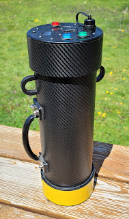
I have for sale a very high-quality, custom built with an extreme attention to detail, no-expense-spared, no-corners-cut "kind of deal" VNA. This an absolutely completed N2PK VNA set ready to be connected to a computer and DUT - not a bit of additional work is needed. It is for somebody who wants to quickly get a hold of a fine N2PK VNA and own a superb, completed unit and a set of accessories, without the hassle of the DIY project. This is not something, quickly slapped together and shoved in a box - it is an accurate and capable instrument, built with passion and skill. It is probably as good as it gets, short from a CNCed enclosure or an "oven"-ized unit.
Included in this sale:
- N2PK VNA based on Ivan Makarov's v4.3 PCB, ALL of the components are from Makarov's/Paul's original BOM (no substitutions), Master Oscillator is by Connor-Winfield (not the VF pictured). Both detectors are shielded in separate RF cans. Inputs and outputs of each detector are also internally shielded from each other inside each RF can. Both DDS chips and the MO are all heat-sink cooled (MO is using separate heat-sink). Everything is hand-soldered, component placement and soldering work is impeccable (30 years of experience). High-quality MA/COM gold-plated SMAs on the main PCB.
There was no rework during the building process whatsoever or any need for troubleshooting - everything worked the first time.
The Internal Multi-voltage Power Supply module is custom made (I have designed the PCB layout) using switching and linear voltage regulators. Shielded in a separate RF can and with extra noise filters, over-current and over-voltage protections - provides highly regulated and clean power.
The thermal design is using the extruded aluminum enclosure as a giant heat-sink, stabilizing the internal enclosure temperature.


Everything is modular and interconnected using quality gold-plated connectors - front and rear panels, Main VNA board and Internal Power Supply Module - all can be easily disconnected from each other and removed if necessary. All you need to take the whole instrument apart is an allen key and a SMA wrench. All connectors are properly marked to avoid connection mistakes. The Main VNA PCB ground layers are connected to the chassis by 2 special edge mounted copper-beryllium clips - it is a solid friction mount for the PCB assembly.
Dynamic Range is between 120 dB and 130 dB as expected - on request I can provide noise floor plots for both detectors. Frequency range is the typical N2PK 0.05 to 60 MHz. Minimum voltage supply required at the rear DC jack (PS is using linear LDO regulators) is 13.4V (maximum recommended +18V).

The presence of the two main power supply voltages +12V and +5V is indicated by LEDs
- External USB to Parallel interface /w USB to Mini USB cable. The v4.3 VNA PCB has a parallel port interface and with this additional interface module it can be used with any USB enabled computer. The interface drivers are 100% compatible with myVNA software (the USB`
interface EEPROM is already programmed, only drivers need to be installed on the host computer). This converter is specifically designed for N2PK VNA by the creator of the MyVNA software. It is mounted in a separate die-cast aluminum enclosure for RFI shielding and it is allowing the user to effortlessly select Parallel Port or USB interface use.
- The standard N2PK T1-6T Reflection Bridge /w BNC connectors (Female silver-plated BNC DUT port). Mounts directly onto the VNA front panel connectors.
- N2PK VNA RF I/V Sensor. Uses only one VNA detector, feeding I and V samples from the DUT. Employs Makarov's PCB and ferrite cores for both transformers. Extensive internal RF shielding between components. Mounted in aluminum enclosure, native stainless steel SMA (f) connectors and HQ SMA-to-BNC between-series adapters already installed. Plugs directly into the VNA Accessories connector and mounts right on the front panel VNA connectors.
- Custom External Power supply - small, low-noise, regulated and filtered linear 16V power supply. Using external PS reduces internally generated heat and RF noise.
- A set of Open, Short and Load (50 ohm) Male BNC cabliration standards ,an additional male BNC connector for use as a Test Fixture (same reference plane as the calibration standards) - just solder DUT directly. The Load standard is using special high-frequency, high-precision resistor.
- Custom, High Quality, shielded PC Parallel Port to N2PK VNA cable - extra long (12ft)
Price is set to $995 and includes insured USPS Priority shipping. Shipping to Continental USA ONLY! No international buyers please. Payment can be done by mailing a Cashier's Check or a Money Order only. Will ship in two business days of receiving the funds.
If you have any questions or you are interested in buying this unit - do not hesitate to contact me - ae1s (at) arrl.net
I have built two N2PK VNAs - a smaller enclosure, BNC version with external USB converter (this is the one I am selling) and a larger Type-N connectors version with an integral USB. It seemed as a good idea at the time to build two units - one for portable / field use and another unit for my lab work-bench. As it turns out - only one unit covers completely my VNA needs and I decided to sell the extra one in order to raise funds for some future projects I would like to dive into. It just doesn't get used enough and it is sitting on my shelf, while somebody could have a good use of it.
As I stated above - no expense was spared when building this VNA - I was building it for myself and not in a hurry - I wanted to have the best, the N2PK design has to offer. I've used the highest quality components and materials I was able to put my hands on and took me months to complete it. The built process is very well documented here, on my blog - from August 31, 2009 and on. You'll find many pictures and comments regarding this unit.
I am not trying to get rich by all means with this sale, so let me be upfront - the cost of components and materials is somewhere between $700 - $800 (I have Digikey/Mouser/eBay invoices for most of the components and materials). It took me many weeks, if not months to collect all of the parts and build this instrument - many hours of SMD soldering under magnification, painstakingly inspecting every single solder joint, a lot of mechanical work on the face-plates, the semi-rigid coax assemblies and the PS Module, design work (CAD PCB layout for the PS, graphics design for the panels), wiring etc.
Frankly, I can not even put value on the time and labor this project so readily consumed. I think the sale price is fair and if it doesn't sale I won't be incredibly disappointed - I have some mixed feelings about selling it anyway.


2 comments:
Андрей, this is a very beautiful build. I build one myself but didn't manage to place it in enclosure so far. I took inspiration from your build to finish my VNA :)
BR,
Tsvetelin
Здравей Цветелин, I am glad that you found the inspiration to finish your analyzer. Initially I wanted to have two units - a portable and a desktop version. I realized that the desktop version is not that large and it works out fine in portable applications so I kept only one. My desktop build is here - http://blog.kotarak.net/2012/01/my-2nd-generation-n2pk-vna.html
The N2PK is a fantastic analyzer and I don't miss at all the wide band frequency range other analyzers offer as most of the circuits I test are in HF range. Let me know if you have any questions! 73, de Andrey AE1S
Post a Comment