Main differences over my first generation unit:
- built-in USB interface using HSUSB (both VNAs are based on the parallel port PCB ver. 4.3)
- larger enclosure with separate shielded RF deck compartment and PS/USB rear compartment (Hammond 1455T2201, Digi-Key p/n HM905-ND)
- Instrument grade, stainless steel precision Type-N and SMA front panel connectors (Amphenol 131-445 / HP-Agilent #1250-1404)
- All internal RF connections are made with Conformable semi-rigid RG-402 coax (Belden 1673A)
 The larger enclosure provides better cooling and thermal stability. I have separated the space into two compartments in order to improve the RF shielding and noise floor. Furthermore, the use of semi-rigid coax requires more space. I must say that working with semi-rigid coax is not an easy thing, even when using hand-conformable type. The connections must be fabricated with a great precision, avoiding re-bending of the coax. I used scrap pieces coax to get the right shape of each link and then carefully followed the shape with the actual coax, bending it only once.
 The front panel is using very-high quality lab-grade (read: very expensive) RF connectors. I also improved on the front panel layout. A front panel LED indicates +5V power to the DDS chips.
 The rear panel with industrial grade Type-B USB connector. The LED next to the connector indicates power to the USB interface. The USB interface board can be powered by the host computer or by the internal power supply (jumper selectable). I also made a small modification to the HSUSB board to incorporate the VNA PWR DETECT signal directly on the board itself. An Accessory connector is installed for connecting the S-parameter test set, RF-IV test head or any of the two transverters. It is a 6 pin connector with all necessary control signals and +9V power for the accessories.
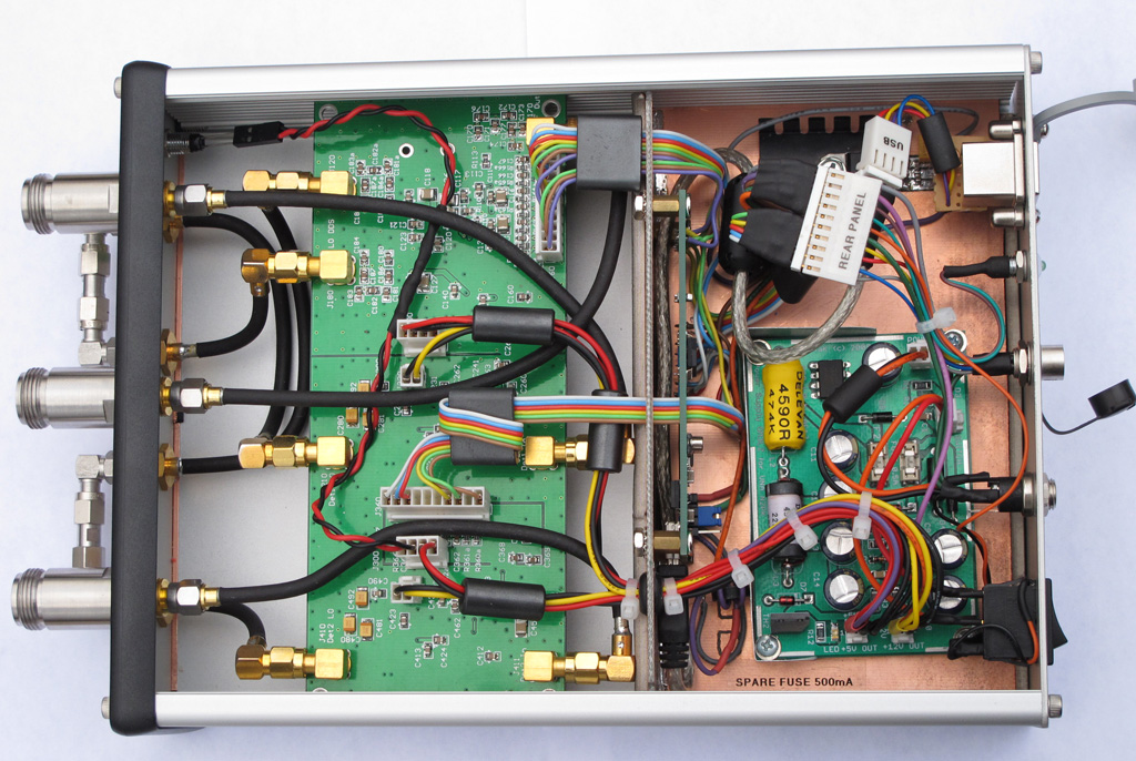
 The power supply mounting bed. The N2PK VNA power supply provides +5v (using a switching regulator), +9V and +12V (linear regulators). There are "crowbar" type over-voltage protections for both, the +5 and +12 V as well as extensive filtering and power conditioning. This picture is with the top RF shield of the PS board removed. The HSUSB board is mounted vertically using stand-offs, on the back wall of the RF compartment shield. The linear regulator and heatsink next to the PS board is for +9V line going to the ACC connector.
The PS mount was constructed by soldering two pieces of copper-clad FR4 PCB material.
On the bottom I mounted copper-beryllium contact clips for better grounding to the aluminum enclosure. When installed, it is a tight fit in the aluminum enclosure, effectively shielding the VNA board from the switching PS and USB interface board. Using such mount, I was able to install everything in the enclosure without drilling any holes and using external screws - it is pure aesthetics but the VNA does look sharp that way.
 The noise floor of Detector 1 is slightly better than -120 dB for the most part (0.05 to 30 MHz it is about -122 dB).
 In addition, I made a reflection bridge using SMA ports and SMA-to-N adapters. Initially, I was going to built it with flange Type-N connectors but these are more involved (5 holes, 4 screws each) to install and the Bridge becomes too "rigid" while being mounted on the VNA ports. The bulkhead type SMA (f) requires just a single D-hole to install and in general the SMA port gives more flexibility. The SMA connector is not the optimal solution for heavy front panel use but this is not the case as the SMA(m) to male Type-N adapters will be almost permanently installed. I soldered the back of each SMA to a brass strip for improved grounding to the chassis and PCB. An additional SMA (f) connector for low impedance termination (used for measurements below 0.5 MHz) was also installed and connected with a short pigtail of RG-405.
 I used a stainless steel, heavy duty SMA on the DUT side as it will see more connect-disconnect cycles than the VNA side SMAs but it required a cutout in the PCB and a small brass plate to solder the ground plane.