I decided to build my own Gamma Spectroscopy detector - I needed a second one to experiment with coincidence counting and realized that it was not going to be very difficult to assemble the detector myself. In addition, I wanted to use a larger crystal for this build and have a detector with a bit higher efficiency than my other two detectors.
I had a damaged Scionix-Holland 38B57 (from Exploranium GR-135) laying around. These detectors can not be repaired due to their integrated design (the bare scintillation crystal and the PMT are glued together before they are sealed) but this unit was going to provide me with a few usable parts that I managed to salvage - namely the Voltage Divider PCB, some Mu-Metal shielding and the stainless steel enclosure with an end-cap.
The main components for the new detector were procured from eBay.
Photomultiplier Tube
I opted for Hamamatsu R980 PMT. This is exactly the same tube used in the Scionix-Holland 38B57 detector and I am familiar with this tube - I worked with it when rebuilding a couple of 38B57s.
R980 is designed for scintillation counting and gamma cameras and it is optimized for use with NaI(Tl) crystals. It is a 10-stage photomultiplier tube with 38mm diameter and Bialkali Photocathode.
The datasheet for Hamamatsu R980 can be found HERE
Emission spectra of NaI(Tl), CsI(Tl) and CeBr3, scaled on maximum emission intensity.
Also a typical quantum efficiency curve of a Bialkali photocathode and a Silicon Photomultiplier (SiPm) are shown above.
Wavelength of maximum response for R980 is 420nm which is almost an ideal match for the NaI(Tl) emission spectra.
I purchased the PMT tube from iRad Inc on eBay (Thank you Tom!). The exact model is Hamamatsu R980-19 which is identical to the standard R980 with the exception of the already installed voltage divider board on the back (designed for GE/Gamma Camera).
This tube was made in China, not Japan but I am convinced that it is going to be just as good. Japanese tubes are older, much difficult to find, more expensive and I doubt they will provide enough of a difference to warrant the trouble of obtaining one.
The "business end" of the photomultiplier tube. The dark-brownish coating on the inside of the glass window is the Photocathode. The glass window was thoroughly cleaned with Acetone from any dust particles and fingerprints.
I didn't bother with figuring out the schematics and reverse-engineering the voltage divider installed on the -19 variant. Glancing at the board indicated that the values of the resistors were not what I needed so I decided to scrap the entire VD board for now and removed it from the tube. I will probably look into the board later and see if it can be easily adapted for another project.
Using the PCB from the damaged 38B57, all components were stripped, the board was cleaned from the flux residue and a new set of components were installed with value for R=2MOhm. The resistors I installed are Vishay TNPV12062M00BEEN (Digikey 541-2324-1-ND) SMD 1206 2 MOhm 0.1% 1/4W Thin Film High Voltage resistors.
The filter capacitors are Kemet C1812C103KGRACAUTO (Digikey 399-16777-1-ND) SMD 1812 Ceramic 10nF / 2000V X7R 10%.
All resistors were selected from a larger pool, with an LCR Bridge to closely match their values between each-other and tolerance was somewhat better than 0.1%.
The picture above shows the component placement on the reworked VD of the original 38B57 board - fortunately the PCB layout worked out perfectly and I only had to add a single jumper wire, while using the old pads.
This is the schematic of the "classic" PMT voltage divider I used.
This schematic shows 120 MOhm voltage divider which is more suitable for counting with a battery powered equipment. Due to the higher impendence, lower voltage drop will occur if the HV power supply is rated for lower current.
Normally, for Gamma Spectrometry, 1M / 2M resistors in VD are used with "stiffer", lab-grade HV power supplies (total impedance of 12 MOhm) but I wanted to help a bit the GS-USB-PRO HV circuit so I went ahead with R/2R as 2 Mohm / 4 MOhm VD (total of 24 MOhm). Another option would be using 1.5MOhm resistors as a good compromise.
The voltage divider board installed on the leads of the PMT.
I left the Anode and Cathode leads slightly longer than the Dynode leads as they will serve as connection points for the coaxial cable going to the BNC / SHV connector.
A layer of electrical tape was applied to act as a light shielding and also protecting the tube's glass envelope from being scratched by the magnetic shielding sleeve.
I wrapped the first Mu-Metal magnetic shield around the PMT and covered it with another layer of electrical tape. The Mu-Metal shield is grounded to the Cathode lead of the PMT on the bottom side the PCB.
Shielding is very important as external electrostatic and magnetic interference, including Earth's magnetic field can affect the path of the electrons when when they are just emitted by the Photocathode and to a lesser degree - when bouncing from Dynode to Dynode.
In my design, I use two layers of Mu-Metal sleeves - first layer covers the back of the PMT in the area around the Dynodes and the second layer shields the entire PMT assembly.
Scintillating Crystal
The scintillation crystal - NaI(Tl) or Sodium Iodide doped with Thallium is the "heart" of the detector and extra care should be taken when selecting and purchasing one. NaI(Tl) is by far the most widely used general purpose-scintillator material and produces excellent results for the cost.
The crystal I obtained is 25% larger than a typical 1.5" x 2.5" crystal used in many detectors - the size of this crystal is 40mm x 80mm (~1.5" x 3.1") which should result in a bit better efficiency.
The crystal is encapsulated in a thin aluminum canister with reflective material surrounding it and an optical glass window for interfacing with the Photomultiplier.
The Sodium Iodide is an extremely hygroscopic substance and the crystal must be hermetically sealed or moisture from the air will quickly "hydrolyze" it and destroy it.
My crystal was procured from an eBay seller located in Ukraine.
Looking at the label at the bottom and the accompanied paperwork, it was produced in May 1997 either in Russia or Ukraine.
There are some really high quality NOS NaI(Tl) crystals made in Russia and the cost is extremely competitive even when compared with the new ones coming from China. There is a good variety of sizes to choose from as well.
Unfortunately, some NOS crystals are really old, now with leaking seals so one should be sure of the crystal condition before purchase.
This is what a good crystal should look like, when viewed thru the optical window - completely clear with no cracks or fractures, no yellowing due to moisture / age, no stains on the reflective coating, no cloudiness in the crystal itself, etc. It pretty much should look as if there is nothing in the canister (speaking of "crystal clear" :-).This one looks absolutely clear and pristine!
There is a lot of pure junk on eBay too! Sometimes sold for absolutely outrages prices, I have seen broken windows, broken crystals, yellowed, wet / hydrolyzed and some crystals that are completely unusable for pretty much anything - even counting. I highly recommend that one should request detailed pictures before buying a pricey crystal and to stay away from anything that shows the slightest imperfections - if the window seal or the integrity of the encapsulation canister is compromised, it is just a matter of time before the crystal is spoiled by moisture. Any internal yellowing and cracks will surely result in poor light output, decreased efficiency and lower resolution.
Assembly
Unfortunately, when mating a Japanese PMT and a Russian crystal some difference in the standards is to be expected.
The PMT has 38mm (1.5") diameter while the glass window of the crystal container is with 40mm diameter. The aluminum canister itself has 46mm OD.
This small mismatch should not be a big deal and I don't think that many photons will be lost around the edge. Ideally, the PMT's photocathode area should be exact or larger size than the crystal's window but only 1-2 mm around is not that much of a gap and the wasted area is ~122 sq. mm. A negligible loss in resolution is to be expected. The next size over is a 2" PMT (51mm) which would be a much better fit but I just didn't want to deal with the implications - fabricating larger housing, building larger lead castle shielding, etc.
In addition, I use my detectors mainly in a head-on application and this results in most photons generated alongside of the main optical axis of the assembly rather than from the side walls. With the reflector surrounding the crystal the probability of losing low-energy photons in the narrow gap is fairly small.
In order to couple the different size devices, I designed an adapter in TinkerCAD which serves a double purpose - it centers the PMT over the glass window of the crystal canister and also serves as a reflector to bounce back any photons escaping from the size-difference gap and the side glass of the PMT's photocathode window.
The adapter ring 3D-printed with resin using SLA 3D printing technology.
The ID of the PMT side is 38mm and of the crystal side is 46mm. There is a 4mm of tapering in the middle which is painted with ultra-bright white paint.
The 4 extended "fingers" of the crown are used to glue the adapter to the crystal canister with RTV sealant.
Optical interface compounds ensure that there is minimal reflection / refraction from each glass-to-air surface and the photons will pass between the crystal and the Photocathode of the PMT efficiently, with maximum light transfer and minimal loss.
These compounds are usually silicone-based - a grease is sold by iRad Inc. and I found that RC Car differential fluid (60 000 cSt or higher), which is extremely viscous, much thicker than honey and it barely flows, while crystal-clear at the same time works extremely well.
Coupling with silicone grease.
A dab of the optical compound is applied in the center and then the PMT is gently pressed with a circular motion to squeeze out all of the air bubbles, the excess grease and to spread it evenly, leaving a very thin film between the two glass surfaces.
I tested also the heavy silicone-based RC Car differential fluid (100 000 cSt) and this is what I currently use as I noticed a very slight improvement in resolution.
Both components are pressed together and secured with a tight wrap of electrical tape, binding them firmly together.
Eight vertical strips of tape are stretched, pulling both components together and multiple turns of tape around the perimeter secures and seals everything.
It is important that all of the excess silicone grease is thoroughly cleaned in order for the adhesive tape to establish good and tight coupling.
(!) No excessive force should be used as the interface between the two glass surfaces is just a thin film of silicone fluid and damage can occur if pressed too hard.
The second layer of Mu-Metal magnetic shielding.
I soldered the Mu-Metal sheet into a tight-fitting sleeve which was placed over the PMT and the sleeve was connected to the the Cathode lead of the PMT, just like with the first layer of shielding.
This second sleeve covers the entire length of the tube and shields the area of the Photocathode where the electrons, just emitted and heading for the first Dynode have minimum energy and are easily deflected by external magnetic fields.
There is an "edge effect" where the shielding effectiveness drops at each edge of the cylinder. This means that ideally, the Mu-shield should be overlapping and extending beyond the boundaries of the PMT.
In my design the condition is met at the dynode side but the shield is a bit short on the photocathode side - it ends at the photocathode plane while in reality, it should be extending beyond the photocathode and overlapping the crystal. I don't expect this to be an issue of any significance and it will keep the maximum diameter of the detector down.
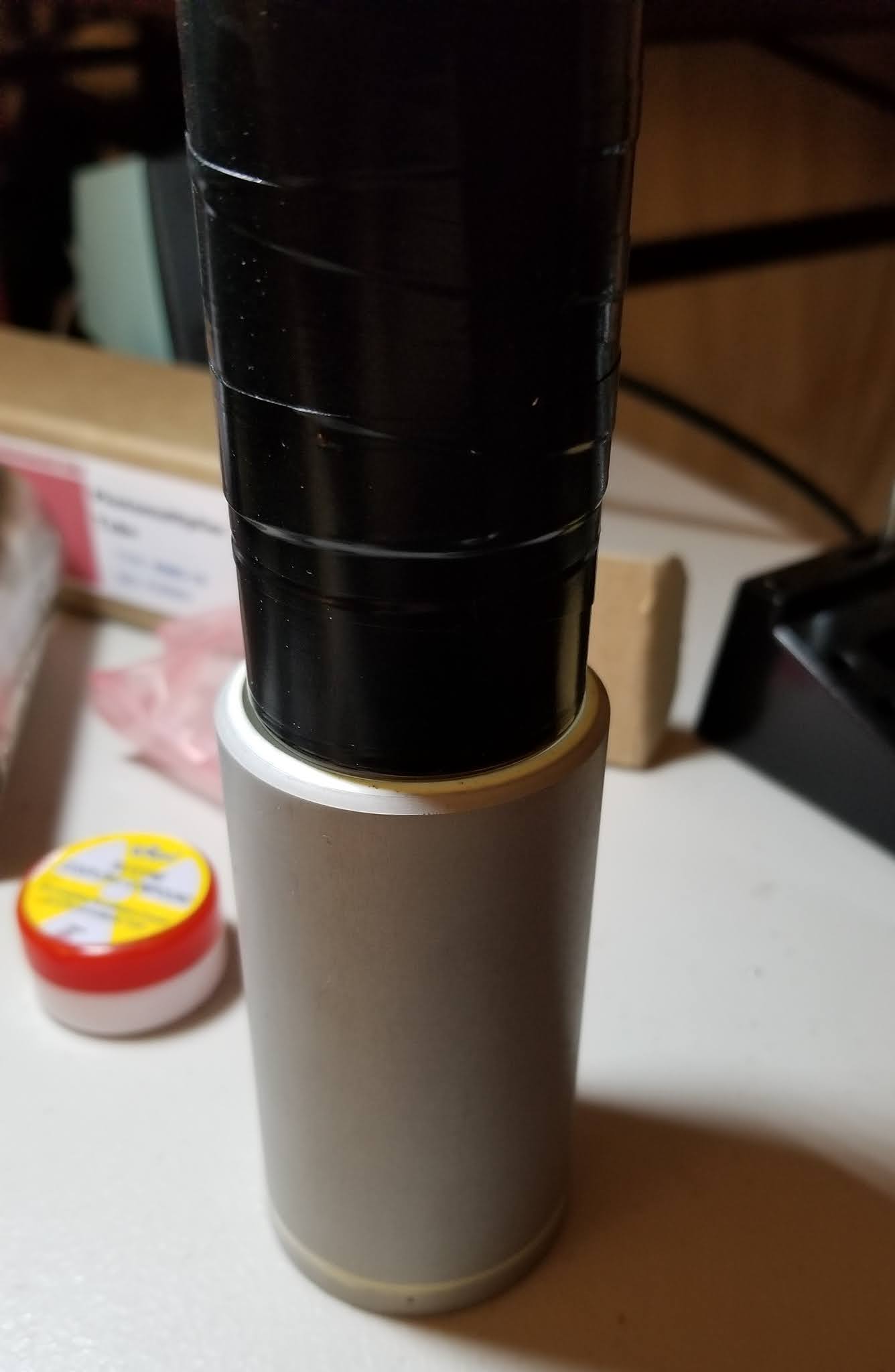
The stainless steel cylindrical enclosure, left over from the damaged 38B57 detector is placed over the PMT assembly and secured to the crystal's encapsulation canister with electrical tape. This worked perfectly well as the PMT is a bit shorter than the enclosure and leaves enough room in the back for the end-cap, the coax interconnect and the coax connector.
Although this enclosure does not cover the crystal canister, it does provide additional shielding and mechanical stability / protection for the PMT and nicely finishes the entire assembly, giving it a very solid feel.
Plenty of space is left for the coaxial pigtail and the connector installed on the aluminum end-cap.
I decided to go for a single cable VD circuit which provides both - PMT's high-voltage bias and transfers the signal pulses to the driver.
Should one chooses to use the two cable design, both connectors HV and Signal can be installed on the cap - there is a plenty of room.
The Kings 1704-1 SHV (Safe High-Voltage) type connector is rated for up to 5000V / 5A and even though I am powering the PMT with only 600-800V, it still makes a more reliable and safe connection at these high voltages.
These connectors are not very common but this also prevents connection errors as they would not mate with standard BNCs. The main disadvantage is the need for special cables - again eBay is a good source for complete SHV cable assemblies.
The coaxial cable shielding, Mu-Metal shielding and the stainless steel cylindrical enclosure are all connected together and grounded to the PMT's Cathode lead.
The center conductor of the coax is connected to the VD's Anode lead.
A 2" heat-shrink tubing is applied over the crystal's encapsulation and partly covers the stainless steel PMT enclosure.
The heat-shrink tube secures the assembly better, covers and seals the tape and provides some mechanical shock protection to the thin-wall aluminum canister of the scintillating crystal.
I used very thin heat-shrink which did not require much heat to activate in order to avoid excessive heating of the crystal. The heat-shrinking was done it short burst with time for cooling to prevent the crystal's temperature from raising and creating a thermal shock.
Words of caution (!):
1. Using heat-shrink tubing over the crystal must be done very carefully to avoid overheating and thermal shock to the crystal, which could possibly damaged it.
2. The Photomultiplier tube should never be powered when exposed to daylight or even ambient room light - such action will immediately deplete / destroy the super-sensitive Photocathode. Any testing should be done in a light-tight enclosure, in a complete darkness, with the only source of light being the scintillation crystal. Removing of the enclosure end-cap while the tube is powered could also cause severe light leakage thru the back side of the PMT.
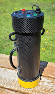
Completed!
The complete detector assembly of DGB-1531.
Overall dimensions (without the connector) are 225mm x 50mm.The black area is the NaI(Tl) crystal and the rest is the enclosure with the PMT and VD.
I shall call it "Da Gamma Bee" (DGB) because of the black / yellow pattern and ability to collect high-energy photons :-)
Initially, the connection to the Gamma Spectacular GS-USB-PRO driver was done with a standard Teflon dielectric BNC type connector but later, I replaced it with SHV type connector for consistency with my other, GS-1525 detector.
This way I can use the same cable with both detectors.
A very quick-n-dirty test shows 6.7% resolution at 650V. (screen capture shows 6.9% due the excited Photocathode by the daylight, right after detector assembly. It improved to 6.7% a few hours later)
Larger crystals tend to have slightly lower resolution but better efficiency - it is a trade off and for NaI(Tl) crystal of this size, I think 6.7% is pretty good.
Basically, the thicker the crystal is, the more scintillating matter there is in the path of the high-energy photon and there is a higher probability for interaction, thus the higher efficiency.
My GS-USB-PRO currently is precisely tuned for the GS-1525 detector and I didn't want to mess with the signal shape filter or the output volume level at this time but I am sure after a few tweaks the result will get even better.
This VD produces slightly lower signal level at the same bias voltage compared to my GS-1525 detector and to compensate for it without adjusting the volume control, I just increased the Audio gain to x1.5 in the software. The pulse width is also a bit shorter than optimal 100uS but this can be easily adjusted with the Shape filter of the Gamma Spectacular unit when I start fine tuning it.
I will also need to determine the optimal bias voltage for the PMT to achieve the best linearity - using Eu-152 or Th-232 source with multiple peaks at different energies and a special Excel sheet this can be done fairly easy.
As a preliminary observation - the background radiation count is higher with the detector I have built (137.5 CPS) when compared to my GS-1525 detector (108.8 CPS). This is a good sign and a significant increase (~26%) in the sensitivity due to the larger crystal volume (~25%) and/or PMT (Hamamatsu R980 (Gain 3.7 x 10^5) vs. ADIT B38B01 (Gain 3.0 x 10^5)) but more testing will be needed with a low activity test sample to precisely quantify the improvement.
The "classic" Cs-137 spectrum obtained with the newly built detector.
Detector Linearity Test plot for 650V, 675V, 700V and 725V PMT bias voltage using a Thorium source / spectrum.
The linearity within the plotted 75V span is excellent overall with best results at 650V. Bias voltage on the other hand, also affects the signal level and while 650V gives me the best linearity results, the signal level is somewhat low causing the spectrum to shift and compress to the left of the energy spectrum. At 700V the signal level is better but the curve begins to bend upwards.
I decided to run the detector at 650V and compensate the signal level using the GS-USB-PRO volume potentiometer as high as it will go in a combination with software x1.5 "Audio Boost" - this restored the correct spread of the spectrum over the a.b.u range with minimal non-linearity.
A good sign the fairly linear result is that in Theremino MCA, after adjusting the Energy Trimmer, the Linearizer sliders barely need to be touched to match exactly the Thorium's multiple peaks with their corresponding energies.
As expected, a minimal adjustment was needed below 50 keV and above 2600 keV but the mid-range sliders were at their default center positions (or very close to). Actually, the linearity turns out to be a bit better than that of my GammaSpectacular GS-1525 detector at 600V.
I must say - It is a very good start! Overall, I am really happy with the end results and I am looking forward to optimizing and tuning the entire setup.
This whole effort is also a proof that if on a budget, one can build a quality GS detector for just a fraction of the cost, normally charged for similar (or lesser) devices by companies catering to the hobbyist market.
It only took me less than a day to build it, once I had all of the parts at hand.