
 Both transverters share exactly the same design and PCB with only a few differences in the BOM - the frequency of the Local Oscillator (180 MHz for the 2m version and 400 MHz for 70cm) and the the components of the Band Pass Filter (different set of components for each filter, changing their frequency range).
I started with the 2m transverter kit from Ivan, VE3IVM. It was an easy and pleasant build - Ivan provided a partial kit - PCB, LO, BPF coils, balun transformer for the bridge, both mixers and a power splitter- the rest of the BOM is from Digikey.
 The top side of the PCB. The 4 coils of the BPF are shielded, each in its own compartment. It is important that they are centered and lifted from the ground plane in order to increase the Q and minimize losses. The other components are the LO, both mixers, RA SMA connectors and the voltage regulators - +6V and +5V. The most time consuming task here is to make and install the shield for the BPF coils - a certain level of precision is required while fabricating the RF shield as the tolerances are not very large. The top cover is soldered during the finalization stage. I used tin-plated brass sheet to make all RF shields - this material is very easy to form and solder.
 Most of the components are installed on the bottom side. Again, a lot of attention is required when building the BPF and the bottom shield for it. After adjusting the BPF, the bottom shield is installed and the filter is checked and re-aligned again as the shield might de-tune it a little. The attenuators are pretty small and should be soldered very carefully. Same thing goes for the 100 Ohm 0604 bridge resistors. The two amplifiers should be soldered carefully to avoid over-heating. Ivan provides specific instructions for installing the variable caps - no flux (or very minimal) should be used and the board must be washed with alcohol or flux remover to avoid mechanical damage to the trimmer capacitors. This picture shows an incomplete and bypassed Low-Pass filter on the low-side output. The jumper is removed and the rest of the components are installed during the finalization stage and after final alignment of the BPF.
![]() This is a plot of the BPF frequency response from the initial alignment of the filter. I was aiming at 143 MHz - 153 MHz range. The BPF filter design allows for almost 10 MHz bandwidth in the 2m band and 20 MHz at 70cm. It can be moved a few MHz up or down from this general range if needed just by adjusting the variable BPF capacitors. During the alignment, it is important to achieve as flat as possible band-pass response and proper shape of the skirts. MyVNA really simplifies the use of transverters and takes care of all calculations - the user must enter the LO frequency and frequency range for the high side and myVNA translates this to the VNA's HF working range, while making a plot in the transverter's frequency range.
This is a plot of the BPF frequency response from the initial alignment of the filter. I was aiming at 143 MHz - 153 MHz range. The BPF filter design allows for almost 10 MHz bandwidth in the 2m band and 20 MHz at 70cm. It can be moved a few MHz up or down from this general range if needed just by adjusting the variable BPF capacitors. During the alignment, it is important to achieve as flat as possible band-pass response and proper shape of the skirts. MyVNA really simplifies the use of transverters and takes care of all calculations - the user must enter the LO frequency and frequency range for the high side and myVNA translates this to the VNA's HF working range, while making a plot in the transverter's frequency range.

 The finalized PCB. Shown here is the completed Low-Pass filter and the RF shielding of the BPF. As Ivan, VE3IVM noted in his build instructions, after installing the BPF shields they will slightly de-tune the filter. As expected, I had to re-align it again. A fence-type shield was installed to divide the up-convert and down-convert paths in order to reduce stray coupling and cross-talk.
 Almost done. I installed a toroid choke on the power line. Ivan has designed the PCB to fit in a compact extruded aluminum box - Hammond 1455C801. The board fills up the space with very little room to spare - just enough for the RF choke. It was a bit tricky to drill the holes for the SMA connectors in both panels so they match perfectly the RA connectors - the board has a small horizontal play which helps it a little. A small piece of conductive RFI gasket material (neoprene covered with metalized fabric) is pinched between the base of the RA SMA conectors and the front aluminum faceplate in order to improve grounding of the aluminum enclosure.
 This is the front panel. The labels on the top row are for Transmission mode measurements and the ones on the bottom - for Reflection. I made the small jumper (needed to configure the transverter for Reflection measurements) out of semi-rigid hand-formable RG-405 coax and used a spacer made from a strip FR4 board to fix the distance between the connectors.. The Hammond box is assembled in a way so the plastic trim for the front and rear panels is on the outside (instead of the "normal" way - between the enclosure and the panel plate). This improves the RF shielding as the end panels are in direct electrical contact with the enclosure - there is no gap.
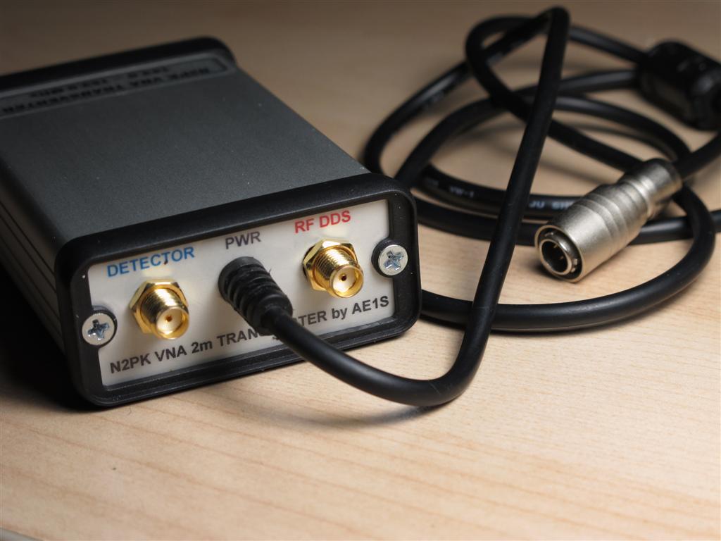 The rear panel and power cable. The Hirose connector for the power cable is the same type that I am using with my RF-IV test head. The accessories connector on the VNA's back panel provides +9V DC and I can power the RF-IV or the transverter directly from there. Two small semi-rigid coax jumpers with Male-BNC to Male-SMA are used to attach the transverter to the VNA's ports. Each of the transverter's ports has a Male-SMA-to-Female-SMA port saver installed (not shown).


 The main reason for matching the calibration reference plane and the mating plane of the VNA test port connector is to allow industrial VNAs to measure whole assemblies and devices, including their connectors. In the N2PK VNA (at least with the original software) the reference plane is assumed to be where the physical OSL calibration takes place. Instead of adding negative offset to move the reference plane back to the mating surface of the VNA's test port connector, it is accepted that the plane is right at the rear surface of the calibration standard connector (the location of the actual Open-Short-Load). The error introduced by the electrical length of the pin inside the connector is not that great at lower frequencies - for instance, assuming teflon dielectric (VF ~70%) in a standard SMA connector used for a home-brewed calibration standard, an offset of 5 mm will yield about 0.5 degree phase error @60 MHz. Commercial calibration standards use air dielectric, but this puts greater mechanical requirements during the fabrication process. By calibrating the VNA so the reference plane is on the back of the cal connector and fully exposed, it is more convenient to measure a single component but it means that the DUT test fixture should be made of (or at least include) the same type connector as the one used for the home-brewed calibration standards in order to maximize the accuracy. The setup can be as simple as the component (DUT) is just soldered on the back of the "test fixture" connector, while measures are taken to minimize external error (minimal lead length). With SMDs, this approach works well as the device is practically located directly at the "reference plane" when the test fixture connector is from the same batch connectors used to make the OSL standards. Another method for calibration is to use the test fixture connector itself for calibration - for OPEN the DUT is simply omitted, SHORT and LOAD are created on the spot during each calibration step and finally the DUT is soldered (Still, stray C for the OPEN must be known)

