This scintillator build is not much different than the others except for using a CsI(Na) crystal and 2" / 51mm PMT.
I understand that people use these posts as a guide when building their own scintillators so I decided to document it as it might provide additional information, which I might have missed in previous posts.
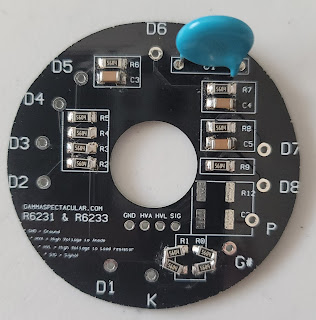
Using Gamma Spectacular PCB for R6231. This PCB is designed for both, single wire (HV Bias + Signal) and 2 wire (HV Bias and a separate Signal line) interface. I populated the PCB for the Single wire interface using R value of 5.6M for the voltage divider. Had to improvise a bit with the 2R resistors between K-G and G-D1 as there was only one footprint per resistor but there are no 11.2M resistors.
Total resistance of the VD is 67.2M.
Voltage-Divider impedance is not a super-critical parameter, but it is important to consider based on the application. For example, with many battery-powered counters and meters where the HV Bias supply can't take much load, high-impedance is preferred as the lower current will reduce the voltage drop. Some low-current PS will drop the output voltage significantly with impedance as low as 60M. In these cases, a total impedance of 120M will work well. High-impedance divider on the other hand will have poor SNR (Signal-to-Noise Ratio) and linearity could suffer as well - for Gamma Spectroscopy with benchtop / lab-grade power supplies, VD impedance of 12M or even lower should work quite well.
For this detector I went "in the middle of the road" with VD around 70M.
Machined PMT rear cap, completed PCB and the PMT ready for the final assembly.
The PMT is a 2" Hamamatsu R6231 - the little brother of R6233. The only difference between the two is really the size - all other specs are the same.
R6233 is one of the best all-around PMTs - I've built more than a dozen detectors with it and absolutely love it - the R6231 should be just as good!
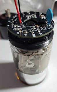
VD PCB installed on the back of the PMT with the two silver-plated, Teflon insulated lead wires.

Installing the MIL-grade BNC connector (Amphenol UG-625 B/U).
There is a wire fed thru a small hole in the cap for grounding the electrostatic shield. Heat shrink tubing is added for extra insulation of the Anode lead and both wires are coiled into "springs" and away from each-other before closing the PMT cap so they don't press on the board and stay away from the components.
The photocathode window was thoroughly cleaned with Acetone and any dust particles were removed using micro-fiber cloth and sticky tape until the glass is absolutely spotless.
The crystal is a "Soviet Era" 40mm x 40mm CsI(Na). Datecode is June, 1991.
CsI is a higher density (4.51g/cm3) scintillation material which makes it more efficient at detecting gamma (better stopping power due to Cesium's higher Z).
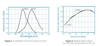
Its light output is 85% when referenced to NaI(Tl) but one big advantage of CsI(Na) when compared to CsI(Tl) is that the emission peak matches perfectly the response of Bialkali PMT photocathode at 420nm wavelength.
CsI(Tl) on the other hand is better suited for use with SiPM as its peak is at 550nm and cutoff at 320nm.
CsI(Na) is also much faster scintillator with decay time of 630ns compared to CsI(Tl) at 3.5us which allows for higher rate detection. Not as fast as the NaI(Tl) with 250ns decay.
Comparison of the emission peak wavelength and temperature response of both types CsI materials.
The light yield is slightly lower with 41 photons/keV Gamma for CsI(Na) compared to 54 photons per keV Gamma for CsI(Tl) but greater than NaI(Tl) with 38 photons/keV Gamma.

My crystal is absolutely pristine - no significant blemishes, no yellowing, no cloudiness. It is crystal-clear (no pun intended).
The glass of the optical interface window was cleaned in the same manner as the PMT's photocathode.
Due to the small difference in diameters between the crystal canister (45mm) and the PMT (51mm), I added a short sleeve from EVA foam around the window area, which will center the crystal during assembly, preventing it from sliding off-center to the PMT. The size difference is very small (~5mm) and there was no need to 3D print a centering collar.
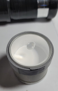
A drop of high-viscosity (100K cSt) silicone fluid is added as optical interface between the two glass surfaces to minimize reflections and refractions by eliminating the air gap between the two glass windows. The silicone oil's refractive index is around 1.41 which is close to the 1.46 refractive index of the borosilicate glass of the PMT.
PMT and crystal are put together and the silicone fluid interface is distributed evenly between the two glass surfaces with repeated, overlapping, wide, circular motion until it becomes a very thin and even layer. The extremely high viscosity of this layer and surface tension prevents it from "running" and it will stay permanently in place.
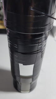
Strips of vertical electrical tape are used to pull together both, PMT and Crystal with some tension. The tape is stretched during application, and it exerts constant pressure between the two parts ensuring a firm contact. With this small diameter PMT 4 long strips (which loop under the crystal) are sufficient.
Both, crystal and PMT are then wrapped multiple times, around, with special focus on the interface zone so it becomes one tight package.
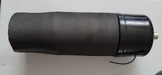
After completely wrapping the assembly with multiple layers of electrical tape, I added a sleeve of EVA (Ethylene-Vinyl Acetate) foam to serve as mechanical shock protection and thermal insulation for the assembly. EVA foam is a very dense closed-cell foam and does great job for both applications.
The front face of the crystal is also protected by a disk of EVA foam, glued to the crystal's foam sleeve.
Needless to say, the assembly is 100% light-proof.
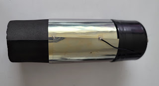
The magnetic / electrostatic shield is added as a two-turns sleeve of special Mu-Metal sheet, spot-soldered closed, and the grounding wire is then soldered to the sleeve. The sleeve overlaps the photocathode area and into the crystal canister by about 5-7 mm.
Second EVA foam layer for even more shock protection of the glass-envelope PMT goes on top of the magnetic shield.
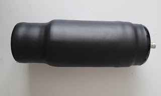
After completing the entire assembly, the final protective layer of heat-shrink tubing is applied.
This is probably the most critical and dangerous part of the assembly process as overheating the crystal can easily cause it to crack. Crystal temperature should not be increased too rapidly. Heat was applied in short burst (with cooling time between them), which allowed the heat-shrink to heat up rapidly but not to transfer a lot of heat at once to the crystal.
Heat-shrinking is not "a must" but provides a nice finish, serves as an additional protective, abrasion / scratch resistant layer and keeps both components - crystal and PMT firmly together.
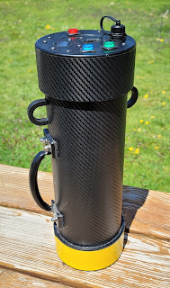
Just as expected, the resolution is not bad at all and spectrum looks pretty good!
Running the detector on 600V PMT Bias. For Cs-137 at 662keV resolution is 6.2% FWHM.
Theremino's algorithm for automatic estimation of the FWHM resolution seems to be a bit on the conservative side so a more realistic value would be actually around 6.0% - not too shabby for a 30-year-old, Soviet Era crystal I must say.












2 comments:
Hello
Would you be kind enough to advise me on the material uses on the Heathkit SB200, looks like a brown tape, under the HV components. Enjoyed the SB 200 write up.
Many thanks.
Charles
W5cry
the polyamide tape is called Kapton tape - you can obtain it from a variety of sources - Amazon, ebay, etc . Just search for "Kapton tape". It has very good high-temperature and electrical resistance and stability.
Here is an example source for the tape - https://www.adafruit.com/product/3057 but you can find it in different thickness and width. Kapton foil without adhesive layer is also available - that's what I use to cover the coils in the SB-200 kit.
Post a Comment