
 This picture shows the box with a bushing for the control cable and the 3 bulkhead female SMA connectors. These connectors require a D-hole to prevent unwanted rotation. Initially, I was going to install male BNC connectors but decided in favour of the SMAs. They require less mounting hardware and I can always use adapters to BNC or N type connectors. In addition, the enclosure is small and installing regular 4 screws bulkhead connectors will prove to be a headache.
 On the inside I installed two L-shaped supports / rails (formed out of tin-plated brass sheet) to create a "bed" for the PCB and a good solderable ground connection for the SMAs.
 On the bottom of the box I placed a piece of FR4 fiberglass PCB material (I etched completely both copper layers using a mixture of Hydrogen Peroxide and Hydrochloric (Muriatic) Acid (1:2))
This board serves as an insulator and also acts as a spacer in order to raise the PCB from the bottom of the box and bring it closer to the bulkhead connectors. The two L-shaped tin-plated side rails go on the top of the fiberglass spacer board holding it into place. The RF-IV PCB goes on top of these rails.
 The RF-IV PCB is installed in the aluminum enclosure. Small ferrite toroid is used for RFI suppression on the control / power lines. The RF DET SMA is connected to the PCB using a short piece of UT-085 semi-rigid coax. Small pieces of silver-plated jumper wires (in teflon sleeves) are connecting the PCB RF ports (RF DDS and DUT) to the bulkhead SMA connectors on the box. I was trying to keep the jumpers as short as possible. Unfortunately, with this enclosure I can't use RA PCB mount SMAs. The outer edge of the PCB's ground plane is soldered directly to the tin-plated brass sides (the L-shaped side rails on each enclosure side with SMA connectors installed)
 I used tin-plated brass screens to create the internal RF shielding. It is important that there is a good RF screening between the RF DDS and DUT ports. Each sampling transformer has its own screened compartment. The L-shaped rails on the two sides with the RF connectors were very convenient points for mounting the screens - I just soldered the RF shield elements to the sides.
 This picture shows that the internal screening is raised about 1-2 mm from the PCB, allowing enough clearance from the components and signal traces.
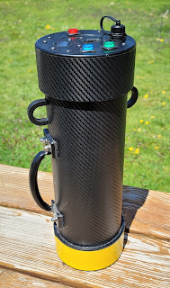
 Picture of the completed RF I/V sensor. This is the "side-up" for Detector 1 use but it can be used with either detector - exactly the same way the reflection bridge is used: just flipping the box and installing it on Detector 2 port (the reverse side of the box is marked for Detector 2)

1 comment:
Blogs that have quality information like this are as precious as gold. You have given me much to think about in this blog. Thank you.
Post a Comment