Friday, February 5, 2010
10 000 visitors and counting
Two years since I first published my SteppIr BigIR Mrk III dissection / review page , the web counter is at 10 000 visitors (only unique IPs are counted). It is a small anniversary and makes it worth all of the effort to create the web page! Enjoy!

Thursday, January 28, 2010
It's a boy!
For lack of better words - the happiest day in my life! Today, Jan 28, 2010 at 4:26 Eastern Time my first harmonic - Vichren Andrey-Endri Stoev was born! He is 9 lbs 3 oz and 21 inches tall. Absolutely a MIT (or Cal Tech - have not decided yet who is going to have the honour ;-)) material - one can tell from first sight! (His crib is furnished with the basics - netbook, shortwave transceiver and CW trainer). Mother and baby are doing very well!
Thursday, December 31, 2009
BulbDial Clock
The idea about an "Indoor Sundial Clock" is not a new one. There are many patent applications filed over the years (some dating back to 70s), describing such devices. It is one of those "how come I didn't think of this" type of ideas - simple yet brilliant. David Friedman of ironicsans.com described such device with a nice illustration (he might have come to this idea independently from the other inventors or not, but he is one of the first with a nice visual instead of the boring wording in patent applications). That's how the name of this clock came about - The Bulb Dial Clock. It was only natural, this idea to be picked up by Evil Mad Science and turned into a really nice kit. The kit is based on the Arduino platform, using Atmel AVR controller (ATmega168). When I saw the kit, I knew I had to have it - such a brilliant idea as a very well executed project = a must-have cool gadget!
I ordered the kit from Evil Mad Scientist as soon as it was made available.
 This is the completed PCB assembly. The LEDs of each board must be aligned before the next board is added to the stack. Power supply adapter is provided with the kit. The clock can also be powered with the optional programming cable (USB-TTL-5V) but only if the power supply is not connected. There is no ON/OFF switch. The Z (sleep) button is on the bottom side which is not the most convenient place - I wish the buttons were more accessible.

I ordered the kit from Evil Mad Scientist as soon as it was made available.
 The kit quality is simply superb. Extremely high quality PCBs and components! Everything is absolutely "top-notch", including the nice laser-cut enclosure (available in a few different styles). All components are sorted by type in labeled plastic bags and packed very well. Included in the kit are a few spare parts - LEDs and mounting hardware. The manual is not provided with the kit - it is available for download and it can be printed. A few words about the manual - probably the best kit manual I've seen lately (maybe even over-done) and it beats Heathkit! The kit is designed for beginners and the manual even includes a section on soldering. If you never held soldering iron, you should be still OK - just follow the instructions.
 The build is straightforward. The most tedious part is installing and aligning the 72 LEDs located on 3 PCBs. This is the main BLUE PCB - it includes 30 blue LEDs for the "seconds hand" as well as the AVR controller and most of the components. The clock has 2 seconds and 2 minutes resolution - in other words - the "seconds" hand moves every 2 seconds and the "minutes" hand - every 2 minutes. This is actually not too bad - imagine dealing with 132 LEDs for full resolution - it would be crazy ! When LEDs are switched on, it can be done with "fading" which gives a nice smooth "analog feel" and makes up for the 2 seconds resolution (it actually interpolates the "in between" state)
There is a connector for accessing and re-programming the ATmega chip. I wish they had provided a socket for the IC in the kit. I felt that it is much safer to play with the firmware if the PIC was socketed, so I added a socket. There is also a provision for an on-board IC voltage regulator should one decides to use non-standard power supply. The design is very simple - ATmega168 chip, crystal oscillator (20ppm), a few current limiting resistors, 3 buttons and a charlieplexed matrix of LEDs. The source code for the firmware is open and the schematics are freely available for download - all in the spirit of the Arduino platform. This picture shows the main board with the nice "bulbdial" face installed on stand-offs. There is machined gnomon in the center which casts the "shadow hands" The GREEN PCB is for the "minutes" hand and it has 30 green LEDs. The picture also shows the special laser-cut "LED leads forming tool" . All LEDs need to be pointed downward and aligned to produce nice centered hot-spot. There is an alignment mode in the firmware to assist this task. One should gently bend the LEDs. Sometimes it is necessary one of the solder joints of the LED to be heated with the soldering iron, while aligning the LED body in order to reduce the mechanical stress.
 This the last of the 3 PCBs - the "hour hand" RED PCB. It has 12 red color LEDs.
The little circular board in the center of the picture is the optional ChronoDot. This board contains a high-accuracy real-time clock (RTC) based on the DS3231 chip. This option improves a lot the accuracy of the Bulbdial clock - without it the clock will drift aprox. +/- 2 min per month. With the ChronoDot, the clock will be accurate to +/- 2 minutes per year. This high accuracy is achieved by the built-in 2ppm Temperature Compensated Crystal Oscillator (TCXO) inside the RTC chip. The ATmega firmware will automatically detect if the ChronoDot is installed and will start using it instead of the software timers. One added benefit of the ChronoDot is the 3V Lithium battery on the back of the PCB (not visible)- it is good for up to 8 years and keeps the time even when the clock is powered down.
 This is the completed PCB assembly. The LEDs of each board must be aligned before the next board is added to the stack. Power supply adapter is provided with the kit. The clock can also be powered with the optional programming cable (USB-TTL-5V) but only if the power supply is not connected. There is no ON/OFF switch. The Z (sleep) button is on the bottom side which is not the most convenient place - I wish the buttons were more accessible.
All 3 boards are inter-connected with 10 zero-ohm resistors (jumpers) and held together with threaded stand-offs and stainless steel hardware.
 There are 4 modes of operation - Time Displaying Mode, Time Setting Mode, Alignment Mode and Optional Configuration Mode. The modes are selected by pressing and holding combinations of buttons. Once the clock is powered, it goes into Time Displaying Mode. In this mode the Z button is Sleep ( it turns off the display) and "+" and "-" control the brightness level.
 There are a few different case styles offered with the kit. The case by itself is an optional item. The enclosure is made of laser-cut acrylic for the front and back faceplates and thin, flexible plastic elements for the sides to create the classic "mantle clock" look.
 If all LEDs are properly aligned, the gnomon in the center will cast nice centered shadows in the LED's hot-spots. Because of the height of each LED ring above the face plane and the angle of the LEDs, each of the three shadows has different length much like the hands of a real clock. The kit that I got is with RGB LEDs but it is also offered in a "monochrome version" using only white LEDs for yet another style.
 I just couldn't resist the "geeky" look with transparent front plate to show off the internal construction. IMHO it looks very cool, with a futuristic "tech feel"!

 There are 4 modes of operation - Time Displaying Mode, Time Setting Mode, Alignment Mode and Optional Configuration Mode. The modes are selected by pressing and holding combinations of buttons. Once the clock is powered, it goes into Time Displaying Mode. In this mode the Z button is Sleep ( it turns off the display) and "+" and "-" control the brightness level.
 There are a few different case styles offered with the kit. The case by itself is an optional item. The enclosure is made of laser-cut acrylic for the front and back faceplates and thin, flexible plastic elements for the sides to create the classic "mantle clock" look.
 If all LEDs are properly aligned, the gnomon in the center will cast nice centered shadows in the LED's hot-spots. Because of the height of each LED ring above the face plane and the angle of the LEDs, each of the three shadows has different length much like the hands of a real clock. The kit that I got is with RGB LEDs but it is also offered in a "monochrome version" using only white LEDs for yet another style.

There are 7 user-adjustable brightness levels and even a "white balance mode", where the brightness of each color can be adjusted separately. At the highest brightness level the clock could almost serve as a night light. All of the configuration variables are stored in the ATmega's eeprom space. There is also a user-selectable "rear-projection mode" where the movement is reversed (CCW) in order to be viewed through the back if the clock is equipped with a semi-transparent face.
The Bulbidal clock is a fun project and the resulting clock is just beautiful to look at.
Wednesday, December 9, 2009
A very exciting day!
Today, I got the chance to personally meet and chat with the person who is responsible for my career as a computer engineer - the co-founder of Apple Inc. and the engineer who designed the famous Apple I, ][ and III - Steve Wozniak! The guy is practically a legend! Back in the early 80s when I was teenager, I had a poster of him on my wall. Applesoft Basic was my very first programming language! My second one - Assembler for MOS 6502. The first computer hardware I designed was for Apple II. Currently, Steve is the Chief Scientist of Fusion-IO - company creating a revolution in the data storage technology utilizing nano-flash memory. Today, they announced their partnership with IBM as their ioMemory technology will be used in IBM's family of System X servers.
It was only fair to show Steve how the Future meets the Past as I handed him my Apple II CFFA project card - a SSD (Solid State Drive) based on CF card for the Apple II family. This project was developed by Richard Dreher - a firmware engineer at Cray Inc.
 This is my CFFA 2.0 card - I have 90% of my entire collection of vintage Apple II software on the CF Card! (yes! games too - who can live without a weekly game of Pac-Man or Space Invaders). The CFFA (Compact Flash For Apple) supports directly ProDos and GS OS partitions and also supports DOS 3.3 volumes via Dos Master.
It was only fair to show Steve how the Future meets the Past as I handed him my Apple II CFFA project card - a SSD (Solid State Drive) based on CF card for the Apple II family. This project was developed by Richard Dreher - a firmware engineer at Cray Inc.
 This is my CFFA 2.0 card - I have 90% of my entire collection of vintage Apple II software on the CF Card! (yes! games too - who can live without a weekly game of Pac-Man or Space Invaders). The CFFA (Compact Flash For Apple) supports directly ProDos and GS OS partitions and also supports DOS 3.3 volumes via Dos Master.
Well, the card is now officially "Woz" certified! :-) Steve was very impressed with this piece of hardware (tnx Rich!!) but couldn't resist asking me the question - "Why do you guys, do this? What is it about the Apple II?" My answer was - "I hoped that you'll be one of the few who can understand it, Steve".

 The "Owner's guide" for my Apple IIgs signed in the spirit of "Apple II Forever" :-)
Saturday, December 5, 2009
N2PK VNA - LLC calibration standard
The RF-IV sensor is very useful for performing measurments of high-Q devices. To improve the accuracy of such measurments, an extra calibration step is required - LLC or Low-Loss Capacitor calibration. It "provides reference of impedance with an accurate 90 degree phase angle in place of the 50 Ohm LOAD standard". A good read about the RF-IV method is this Agilent document. There is also a very informative application note from Agilent about High-Q measurements.
MyVNA software allows for this calibration step since ver. 0.47. LLC calibration requires a special calibration standard - capacitor with very low ESR and very high Q (>10 000). Paul, N2PK recommends the use of a few loads which are "impedance of -j50 at the center of frequency range and maybe a 4:1 freq range - i.e. from Fc/2 to 2*Fc" or 3, 10 and 30 MHz for example. "Another option is to use a cap that has about the same reactance as an inductor whose Q is to be measured".
MyVNA software has a built-in model for the ATC 100B series (Porcelain Superchip Multi-layer) capacitors by American Technical Ceramics . These capacitors are ultra-stable, low ESR, High Q and low noise, specifically designed for microwave use. The accuracy of the capacitance value is not extremely critical since the software allows you to enter the frequency at which the cap is expected to have -j50 impedance and correction can be made there. I followed Paul's example and made 3 calibration standards centered at frequencies close to 3, 10 and 30 MHz using standard values available by ATC. The construction technique for the standards is exactly the same as the one I used to prepare my other BNC calibration standards (described here).
 This picture shows the "30 Mhz LLC standard", using two 47 pF (tolerance 2%) ATC 100B capacitors in parallel for a total value of 94 pF (the impedance is -j50 at proximately 33.85 MHz).
MyVNA software has a built-in model for the ATC 100B series (Porcelain Superchip Multi-layer) capacitors by American Technical Ceramics . These capacitors are ultra-stable, low ESR, High Q and low noise, specifically designed for microwave use. The accuracy of the capacitance value is not extremely critical since the software allows you to enter the frequency at which the cap is expected to have -j50 impedance and correction can be made there. I followed Paul's example and made 3 calibration standards centered at frequencies close to 3, 10 and 30 MHz using standard values available by ATC. The construction technique for the standards is exactly the same as the one I used to prepare my other BNC calibration standards (described here).
 This picture shows the "30 Mhz LLC standard", using two 47 pF (tolerance 2%) ATC 100B capacitors in parallel for a total value of 94 pF (the impedance is -j50 at proximately 33.85 MHz).
Wednesday, November 25, 2009
N2PK VNA - RF-IV Sensor
Finding an enclosure for the RF-IV sensor turned out to be a real challenge. As I mentioned before, because of the size and connector locations of the RF-IV PCB, there are not that many off-the-shelf boxes that were a good fit. I wanted a box that will allow me to install the sensor directly on the VNA's BNC ports (2" apart) and with enough height to install the corresponding bulkhead connectors. I was almost ready to go the CNC machine route and fabricate the enclosure out of a solid block of aluminum. I wanted the sensor enclosure to be compact since it is supported only on the two BNC connectors. After some more searching though, the Bud Industries CN-5701 box (Digikey p/n 377-1512-ND) seemed to be a possible candidate. I still had to use a vertical mill machine to remove the little PCB slots on the inside of the aluminum box and make the walls nice and smooth.
 This picture shows the box with a bushing for the control cable and the 3 bulkhead female SMA connectors. These connectors require a D-hole to prevent unwanted rotation. Initially, I was going to install male BNC connectors but decided in favour of the SMAs. They require less mounting hardware and I can always use adapters to BNC or N type connectors. In addition, the enclosure is small and installing regular 4 screws bulkhead connectors will prove to be a headache.
 On the bottom of the box I placed a piece of FR4 fiberglass PCB material (I etched completely both copper layers using a mixture of Hydrogen Peroxide and Hydrochloric (Muriatic) Acid (1:2))
 The RF-IV PCB is installed in the aluminum enclosure. Small ferrite toroid is used for RFI suppression on the control / power lines. The RF DET SMA is connected to the PCB using a short piece of UT-085 semi-rigid coax. Small pieces of silver-plated jumper wires (in teflon sleeves) are connecting the PCB RF ports (RF DDS and DUT) to the bulkhead SMA connectors on the box. I was trying to keep the jumpers as short as possible. Unfortunately, with this enclosure I can't use RA PCB mount SMAs. The outer edge of the PCB's ground plane is soldered directly to the tin-plated brass sides (the L-shaped side rails on each enclosure side with SMA connectors installed)
 I used tin-plated brass screens to create the internal RF shielding. It is important that there is a good RF screening between the RF DDS and DUT ports. Each sampling transformer has its own screened compartment. The L-shaped rails on the two sides with the RF connectors were very convenient points for mounting the screens - I just soldered the RF shield elements to the sides.
 This picture shows that the internal screening is raised about 1-2 mm from the PCB, allowing enough clearance from the components and signal traces.
 Picture of the completed RF I/V sensor. This is the "side-up" for Detector 1 use but it can be used with either detector - exactly the same way the reflection bridge is used: just flipping the box and installing it on Detector 2 port (the reverse side of the box is marked for Detector 2)
 This picture shows the box with a bushing for the control cable and the 3 bulkhead female SMA connectors. These connectors require a D-hole to prevent unwanted rotation. Initially, I was going to install male BNC connectors but decided in favour of the SMAs. They require less mounting hardware and I can always use adapters to BNC or N type connectors. In addition, the enclosure is small and installing regular 4 screws bulkhead connectors will prove to be a headache.
 On the inside I installed two L-shaped supports / rails (formed out of tin-plated brass sheet) to create a "bed" for the PCB and a good solderable ground connection for the SMAs.
 On the bottom of the box I placed a piece of FR4 fiberglass PCB material (I etched completely both copper layers using a mixture of Hydrogen Peroxide and Hydrochloric (Muriatic) Acid (1:2))
This board serves as an insulator and also acts as a spacer in order to raise the PCB from the bottom of the box and bring it closer to the bulkhead connectors. The two L-shaped tin-plated side rails go on the top of the fiberglass spacer board holding it into place. The RF-IV PCB goes on top of these rails.
 The RF-IV PCB is installed in the aluminum enclosure. Small ferrite toroid is used for RFI suppression on the control / power lines. The RF DET SMA is connected to the PCB using a short piece of UT-085 semi-rigid coax. Small pieces of silver-plated jumper wires (in teflon sleeves) are connecting the PCB RF ports (RF DDS and DUT) to the bulkhead SMA connectors on the box. I was trying to keep the jumpers as short as possible. Unfortunately, with this enclosure I can't use RA PCB mount SMAs. The outer edge of the PCB's ground plane is soldered directly to the tin-plated brass sides (the L-shaped side rails on each enclosure side with SMA connectors installed)
 I used tin-plated brass screens to create the internal RF shielding. It is important that there is a good RF screening between the RF DDS and DUT ports. Each sampling transformer has its own screened compartment. The L-shaped rails on the two sides with the RF connectors were very convenient points for mounting the screens - I just soldered the RF shield elements to the sides.
 This picture shows that the internal screening is raised about 1-2 mm from the PCB, allowing enough clearance from the components and signal traces.
 Picture of the completed RF I/V sensor. This is the "side-up" for Detector 1 use but it can be used with either detector - exactly the same way the reflection bridge is used: just flipping the box and installing it on Detector 2 port (the reverse side of the box is marked for Detector 2)
 Wednesday, November 4, 2009
N2PK VNA - Accessory Connector
The VNA software can control different accessories - like the S-Parameter setup or the RF-IV sensor. This means that some extra control signals and power should be available through an Accessory Connector. There are no available pins on the DB-25 connector and in addition it is not a good idea to have power supplied there anyway.
The Accessory Connector must be at least 6 pins if an S-parameter setup will be connected. I am not planing to build one at this time and I need connector with only 3-4 pins for the power and control signal to the RF-IV sensor and possibly a transverters. Most people are using the Mini-DIN connectors (like the ones used for the PS/2 keyboard or mouse) but I am not really fond of these connectors - this type connector does not provide very secure connection and can be easily pulled apart.
The connector I ended up using is the HR10 type (Hirose Electric) Digikey P/N HR1568-ND (female, panel mount) and HR1558-ND (male, plug). This connector is superior to the Mini-DIN. It is available in 4 pin and 6 pin configurations, it is small and it has a very nice locking mechanism.
Not cheap by any means - a pair (male-female) will set you back almost $30 but it is very high-quality product (nice looking too).
 The Accessory Connector installed on the back panel of my VNA. I am using only 3 out of the 4 pins - GND, +9V and RF-IV Cntrl. Maybe one day I'll make a new silk-screen for the panel and will mark the connector appropriately. The dust cap is Digikey P/N HR345-ND.
Update Jan 2012: I am working on my S-parameter test set and I replaced the 4 pin connectors with the 6 pin version. I have 3 male and 1 female 4 pin HR10 connectors in excess of my needs. Price is $10 per connector + postage (~25% off Digi-key price). All connectors are used (were installed) but in pristine condition.
The Accessory Connector must be at least 6 pins if an S-parameter setup will be connected. I am not planing to build one at this time and I need connector with only 3-4 pins for the power and control signal to the RF-IV sensor and possibly a transverters. Most people are using the Mini-DIN connectors (like the ones used for the PS/2 keyboard or mouse) but I am not really fond of these connectors - this type connector does not provide very secure connection and can be easily pulled apart.
The connector I ended up using is the HR10 type (Hirose Electric) Digikey P/N HR1568-ND (female, panel mount) and HR1558-ND (male, plug). This connector is superior to the Mini-DIN. It is available in 4 pin and 6 pin configurations, it is small and it has a very nice locking mechanism.
Not cheap by any means - a pair (male-female) will set you back almost $30 but it is very high-quality product (nice looking too).
 The Accessory Connector installed on the back panel of my VNA. I am using only 3 out of the 4 pins - GND, +9V and RF-IV Cntrl. Maybe one day I'll make a new silk-screen for the panel and will mark the connector appropriately. The dust cap is Digikey P/N HR345-ND.
Update Jan 2012: I am working on my S-parameter test set and I replaced the 4 pin connectors with the 6 pin version. I have 3 male and 1 female 4 pin HR10 connectors in excess of my needs. Price is $10 per connector + postage (~25% off Digi-key price). All connectors are used (were installed) but in pristine condition.
Tuesday, October 27, 2009
N2PK VNA - USB to Parallel interface
I am pretty happy with the Parallel port interface - it doesn't require any drivers and works just fine. For portable applications using my Netbook in the field, I have no choice but to use an USB interface. My Acer Netbook doesn't have PCMCIA slot (for Parallel card) or native parallel interface and the only option to control the VNA is USB. A standard, off-the-shelf USB to Parallel port converter (commonly sold for printer interfacing) won't work. These converters are designed for printers use only and they don't have 100% bi-directional parallel port support. Fortunately, Dave G8KBB designed a very nice interface based on the Cypress FX2 (EZ-USB) USB micro-controller (CY7C68013A).
For my project I used a PCB from WB6DHW. His interface is a nearly identical clone (electrically) of the G8KBB interface. To be honest, I am less than impressed (other words, which I'll save come to my mind ) with the PCB layout done by WB6DHW - it looked like somebody was learning how to design a PCB and used this project as a practice board. I was almost ready to design my own board (G8KBB's board is excellent but his PCBs are not readily available). Don't mean to bash WB6DHW - just expressing an opinion. At the end of the day tho, I decided to close my eyes and got the bare board from WB6DHW because of its low price - fabricating my own board was going to cost a lot more and wasn't worth the effort/money just for a single piece. All components are from DigiKey, including the Cypress chip and the Hammond die-cast aluminum enclosure housing the interface.
 I had to modify (mill) the PCB in order to fit it in the enclosure. The PCB is raised on stand-offs since the Mini-B USB connector along with some other parts are placed on the bottom side. I prefer to have the much sturdier and more reliable USB-B connector but there wasn't an easy way to modify this board. The Cypress FX2 chip is in a package with fine pitch leads but it wasn't that difficult to solder it pin-by-pin under sufficient magnification. There was no need to install any of the other connectors - I just soldered the wires directly to the board. The enclosure is a tight fit and if I had the connectors installed it would have been difficult to manage the wires inside. The most time-consuming part in this project is wiring the board to the cable and the female DB25 connector according to the schematics and the table provided by Dave G8KBB.
 This is the complete interface. It is rugged yet compact - the only delicate part to worry about is the Mini-B connector. The initial setup is a bit complicated - a Vendor ID and Product ID must be written in the EEPROM in order for the USB micro-controller to properly report the interface in Windows. To accomplish this task, a step-by-step procedure and a piece of configuration software are published on Dave's, G8KBB web site. First, special drivers are installed in Windows to get access to the Cypress FX2 chip and the EEPROM address space. Then, using "USB Configure" (by G8KBB), the appropriate IDs are programmed in the EEPROM according to the hardware in use - version of the interface/VNA and current demand (in case the USB port is used also to power the VNA). This setup is one time deal - afterwards the interface is used with its regular USB drivers.
For my project I used a PCB from WB6DHW. His interface is a nearly identical clone (electrically) of the G8KBB interface. To be honest, I am less than impressed (other words, which I'll save come to my mind ) with the PCB layout done by WB6DHW - it looked like somebody was learning how to design a PCB and used this project as a practice board. I was almost ready to design my own board (G8KBB's board is excellent but his PCBs are not readily available). Don't mean to bash WB6DHW - just expressing an opinion. At the end of the day tho, I decided to close my eyes and got the bare board from WB6DHW because of its low price - fabricating my own board was going to cost a lot more and wasn't worth the effort/money just for a single piece. All components are from DigiKey, including the Cypress chip and the Hammond die-cast aluminum enclosure housing the interface.
 I had to modify (mill) the PCB in order to fit it in the enclosure. The PCB is raised on stand-offs since the Mini-B USB connector along with some other parts are placed on the bottom side. I prefer to have the much sturdier and more reliable USB-B connector but there wasn't an easy way to modify this board. The Cypress FX2 chip is in a package with fine pitch leads but it wasn't that difficult to solder it pin-by-pin under sufficient magnification. There was no need to install any of the other connectors - I just soldered the wires directly to the board. The enclosure is a tight fit and if I had the connectors installed it would have been difficult to manage the wires inside. The most time-consuming part in this project is wiring the board to the cable and the female DB25 connector according to the schematics and the table provided by Dave G8KBB.
 This is the complete interface. It is rugged yet compact - the only delicate part to worry about is the Mini-B connector. The initial setup is a bit complicated - a Vendor ID and Product ID must be written in the EEPROM in order for the USB micro-controller to properly report the interface in Windows. To accomplish this task, a step-by-step procedure and a piece of configuration software are published on Dave's, G8KBB web site. First, special drivers are installed in Windows to get access to the Cypress FX2 chip and the EEPROM address space. Then, using "USB Configure" (by G8KBB), the appropriate IDs are programmed in the EEPROM according to the hardware in use - version of the interface/VNA and current demand (in case the USB port is used also to power the VNA). This setup is one time deal - afterwards the interface is used with its regular USB drivers.
Wednesday, October 21, 2009
N2PK VNA - RF-IV sensor PCB
I've completed the PCB for the RF-IV sensor. Now I have to come up with an enclosure. In addition, I have to install a mini-DIN connector on the VNA's rear panel with power and control signal for the RF-IV sensor.


The PCB is very simple and easy to work with. A thing to note is the slightly awkward placement of the RF connectors - it is needed to achieve certain level of port-to-port isolation. There are two transformers, one (on the left) takes the Current sample, the other (on the right) the Voltage sample - this part of the circuit is almost the same as in Larry's N8LP coupler for the LP-100. The DUT is connected to the RF DDS of the VNA thru the current transformer. The RF switches (Peregrine PE4220 ) are controlled by the software and switch the signal path of the samples to the RF DET input of the VNA. While the VNA takes a sample of the current (I), the voltage (V) transformer is terminated with 50 ohm load and vice versa. There is an on-board 3.3V voltage regulator supplying power to the RF IC switches. Only one detector is used in the VNA in this configuration which improves the stability and accuracy of the measurements as both -the I and the V samples are measured by the same detector alternatively at a high frequency. The control signal to switch between the samples is generated by the software and in this case is just looped thru the VNA.

Tuesday, October 20, 2009
VNA plots of my SteppIR BigIR
I posted a number of plots of my SteppIR BigIR Mrk III /w 80m coil on my antenna site.
All plots were generated with the myVNA software. Calibration of the VNA was performed at the far end of the 100ft feedline to tune-out the transformation effects of the transmission line.
The scan was done while the antenna was tuned for minimum SWR on the 20m band.
The graphs can be seen here
All plots were generated with the myVNA software. Calibration of the VNA was performed at the far end of the 100ft feedline to tune-out the transformation effects of the transmission line.
The scan was done while the antenna was tuned for minimum SWR on the 20m band.
The graphs can be seen here
Thursday, October 8, 2009
N2PK VNA - It is a "Lab in a Box"!
I love my new toy! It is so nice to be able to perform all kinds of measurements and tests without begging "that guy with the HP VNA" and be left at his mercy (and free time).
(btw. Here is a link to a very informative document about the VNA basics by Agilent)
 I tested a transmitter low-pass filter (C-511-T by Bell Industries) which claims 80db attenuation at 54 Mhz on its label.
 Plot of the Return Loss of my LMR-600 coaxial feedline going to the SteppIR vertical. The length of the cable is exactly 100 ft (+/- 1 ft). The graph shows a Return Loss of approx. 1.2 dB @ 50 MHz. The actual loss is one half of the measured RL (just one way) or 0.6 dB @ 50 MHz. Times Microwave specs for LMR-600 are listed as 0.5 dB @ 50 MHz per 100 ft. A 0.1 dB difference is insignificant (I have connectors on both ends and I used a BNC-to-N adapter for the measurement). The cable is under ground in a PVC conduit (hopefully watertight) but I can keep an eye on the losses with the VNA.
 Here is another interesting plot. This graph shows the Return Loss of my entire station - from the transceiver antenna connector to the antenna feed-point connector 100 ft away. The signal path includes a RF patch bay, 2 coaxial switches, 2 directional couplers, gas-discharge lightning arrester, ACOM 1000 amplifier, common-mode choke, well over 100 ft of coaxial cable (in transmission line and jumpers) as well as a large amount of UHF and N connectors.
Detailed RF signal path in the AE1S station can be seen in an old post - here
The loss is approx 1.9 dB on 6 meters (again RL/2) and between 0.3 dB and 1.25 dB on the HF bands. Not bad at all, keeping in mind what is on the signal's path!
The two distinctive "peaks" on the graph are caused by the ACOM 1000 amplifier. These peaks represent the self-resonance of a built-in choke in the amp. The good news is that they are located outside of the amateur bands.
(btw. Here is a link to a very informative document about the VNA basics by Agilent)
 I tested a transmitter low-pass filter (C-511-T by Bell Industries) which claims 80db attenuation at 54 Mhz on its label.
As one can see - attenuation is only 63 dB at 54 Mhz with maximum attenuation of 66.5 dB at 57 MHz - that is pretty far from the claimed "80 dB". This screen-grab shows the true beauty of the Dual Detector setup - for example being able to plot the VSWR curve in reflection mode at the same time as the attenuation curve in transmission mode.
 Its not only a VNA - it is a handy signal generator - myVNA software allows you to use it as adjustable signal generator. This picture shows a rough frequency measurement (my scope has current calibration), 14 Mhz - same as the value set in the software. (the oscilloscope of course can't measure with such great resolution as what the software allows you to adjust but gives an idea about the clean sine wavefrom generated by the DDS).

Among other things - there is a vector volt-meter available in myVNA. This image shows the result of -10 dBm output measured thru a variable precision attenuator (set to 8dB) at 6 MHz : -18.0026 dBm. I'd say pretty accurate! The vector voltmeter can use both ADC at the same time for measurements and display the phase difference as well.
 Plot of the Return Loss of my LMR-600 coaxial feedline going to the SteppIR vertical. The length of the cable is exactly 100 ft (+/- 1 ft). The graph shows a Return Loss of approx. 1.2 dB @ 50 MHz. The actual loss is one half of the measured RL (just one way) or 0.6 dB @ 50 MHz. Times Microwave specs for LMR-600 are listed as 0.5 dB @ 50 MHz per 100 ft. A 0.1 dB difference is insignificant (I have connectors on both ends and I used a BNC-to-N adapter for the measurement). The cable is under ground in a PVC conduit (hopefully watertight) but I can keep an eye on the losses with the VNA.
 Here is another interesting plot. This graph shows the Return Loss of my entire station - from the transceiver antenna connector to the antenna feed-point connector 100 ft away. The signal path includes a RF patch bay, 2 coaxial switches, 2 directional couplers, gas-discharge lightning arrester, ACOM 1000 amplifier, common-mode choke, well over 100 ft of coaxial cable (in transmission line and jumpers) as well as a large amount of UHF and N connectors.
Detailed RF signal path in the AE1S station can be seen in an old post - here
The loss is approx 1.9 dB on 6 meters (again RL/2) and between 0.3 dB and 1.25 dB on the HF bands. Not bad at all, keeping in mind what is on the signal's path!
The two distinctive "peaks" on the graph are caused by the ACOM 1000 amplifier. These peaks represent the self-resonance of a built-in choke in the amp. The good news is that they are located outside of the amateur bands.
... and I am just scratching the surface of this great instrument!
Wednesday, October 7, 2009
N2PK VNA Calibration Standards
Proper calibration is absolutely essential for high accuracy measurements.
Here are some notes on the calibration standards for the N2PK VNA. Initially, I've made my own Open-Short-Load-Thru kit. My VNA is equipped with BNC connectors, so I used "clamp type" male BNC connectors for large diameter coaxial cable (such as LMR400/RG-8) to house my calibration standards. I also wanted to have some reference calibration standard to compare against.
 Final touch - heat-shrink tubing provides color-coding and nice finish.
 This is my full set of (m) BNC calibration standards - in addition to the OSL and LLC standards, I made some extra loads (12.5, 25, 75, 100 and 200 ohms) to aid calibration of other instruments besides the VNA.
Here are some notes on the calibration standards for the N2PK VNA. Initially, I've made my own Open-Short-Load-Thru kit. My VNA is equipped with BNC connectors, so I used "clamp type" male BNC connectors for large diameter coaxial cable (such as LMR400/RG-8) to house my calibration standards. I also wanted to have some reference calibration standard to compare against.
 I was able to acquire (tnx to eBay) a precision commercial VNA calibration kit at very reasonable price. I did some comparison between my home-brewed calibration standards and the Maury Microwave VNA Kit (MMC) - good for VNA calibration DC to 18GHz.
 I wanted all of my cal standards to use the same type of housing in order to easily maintain the same reference plane. Looking at the commercial standards - that's not case - the shells are different size but the reference plane inside must be the same.
As expected, the home-brewed Open and Short standards (which are fairly easy to fabricate), when compared to the expensive commercial standards seem to be pretty close. The Short standard must have low inductance and the Open - low capacitance. Looking at the MMC Short standard - it seems to be made out of one piece of metal for the center pin and the ground shell - the electrical short occurs at the far end of the center pin right at the back-face of the actual connector and the pin's length seems to be shorter than the normal N-connector center pin. The commercial MMC Open load has longer center pin attached to a dielectric disc in the back of the housing but maintains the same "reference plane". The story is much different for the 50 Ohm Load standard. I made two different Load standards using different components (bulk-metal foil resistor and edge-trimmed precision thin film resistor - both rated for high frequency use and optimized for minimal self-reactance) and different construction techniques. Both Loads turned out to be not as good as the MMC Load (which I kind of expected) but the Load with the expensive bulk-metal foil resistor seems to be worse than the thin-film one. I suspect the difference is due to the construction and the much larger SMD component.
In addition, I tested the combination of a Male BNC-to-female SMA adapter + home-brewed SMA Load (housed in RA male SMA connector shell, /w edge-trimmed thin-film resistor) was much closer to the commercial MMC Load and actually quite acceptable.
I'll be trying yet different construction technique for the BNC Load standard. The main challenge with the BNC Loads is the installation of the SMD resistor. The center pin of the BNC is not captive, and it needs to be fixed somehow in order to remove any mechanical stress form the resistor. So far I have not used any glue or epoxy in my cal standard constructions, but I think it is about time to try it.
 Here is the 50 Ohm LOAD standard using a Vishay FC series, high frequency precision (0.1%) 0603 SMD resistor - Digikey p/n FC0603-50BWCT. This size resistor is a perfect fit between the barrel and the center pin. The center pin of the connector is trimmed down, and the resistor is soldered in place.
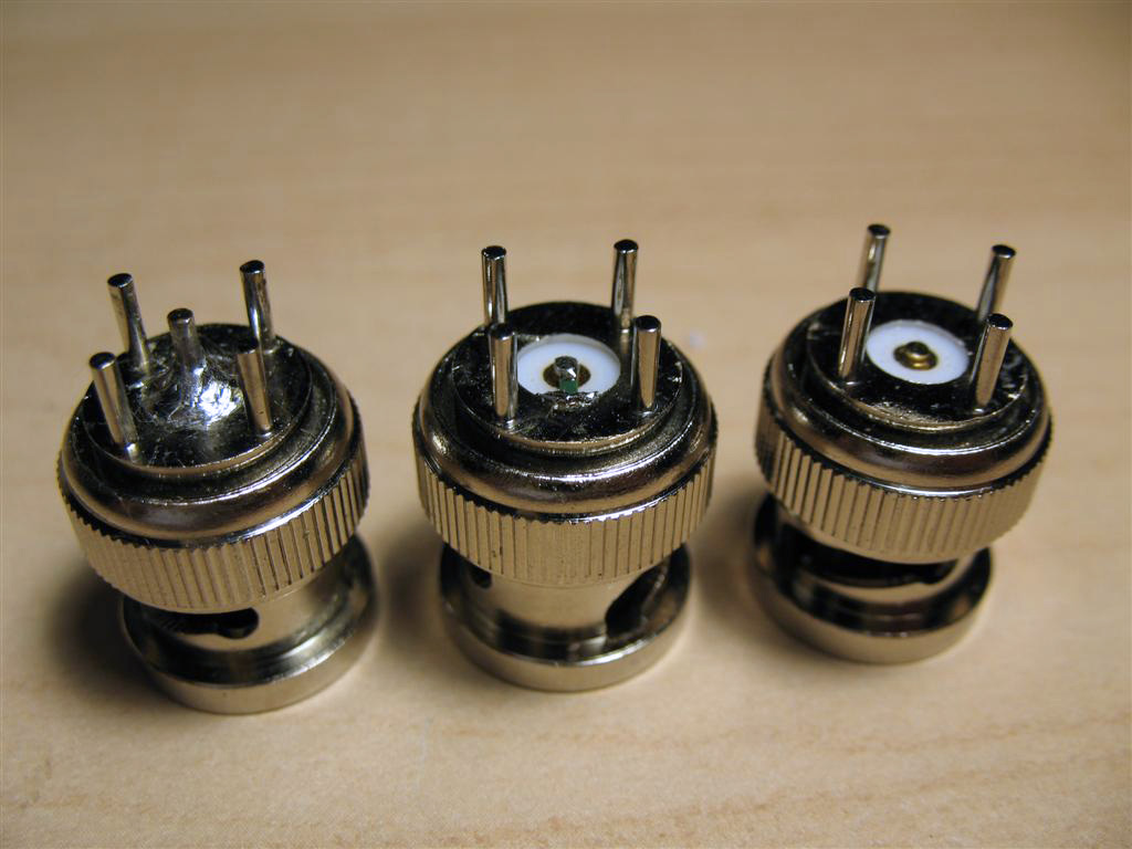 The other two standards - OPEN and SHORT were very easy to make! One should be careful when soldering the SHORT standard not to melt the center insulator with excessive heat (I used a water bath during soldering). On the OPEN standard the center pin must be trimmed down to keep the reference plane the same across all 3 standards.

In order to create RF shielding, provide mechanical protection and facilitate easier handling, I prepared 3 short pieces (~1 cm length) - 2 made with brass tubing (Stock #137, K&S Engineering, 7/16" (11.1mm)) and one of same diameter plastic tube (used for the OPEN standard). I soldered each piece on the inside to the 4 ground pins of the SHORT and LOAD BNCs. Closed-cell foam was used create an endcap for each barrel. The LOAD standard was closed on the back with additional RF shield - tin-plated brass disc, soldered to the inside wall. The body of the OPEN standard was made with the plastic sleeve and glued to the 4 BNC pins - the reason for using plastic is to reduce stray capacitance, caused otherwise by a brass sleeve.
 Final touch - heat-shrink tubing provides color-coding and nice finish.
 This is my full set of (m) BNC calibration standards - in addition to the OSL and LLC standards, I made some extra loads (12.5, 25, 75, 100 and 200 ohms) to aid calibration of other instruments besides the VNA.
Update 2011: The excellent article by William Highton on standard definitions just confirms the fact that BNC connectors make poor calibration standards for ultra high frequencies (500 MHz and up). The home-brewed BNC standards are perfectly fine for the N2PK VNA with its max 60 MHz frequency, but I would not use such DIY kit with commercial GHz VNAs. The standards described above are intended for use with N2PK VNA. Using the same construction method but using different connector - SMA or N type will yield better accuracy with DG8SAQ VNWA or N2PK with N or SMA connectors.
Tuesday, September 22, 2009
N2PK VNA - Some initial plots
 Quick sweep (3 to 29 MHz) of my G5RV clearly shows the low SWR points. It also reminds me that I need to do some minor tuneup of the antenna. The red vertical cursor is at the CW portion of the 20m band - the other SWR dips are in agreement with what should one expect from the classic G5RV. A VNA makes the ultimate antenna analyzer! One extremely valuable feature is the ability to perform calibration at the end of the coax / antenna feed point thus removing the impedance transformation effect of the coax from the measurement! It is like having the VNA connected right at the antenna feed point. (A good overview of various antenna analyzers and designs (incl. N2PK) can be found here )
The noise floor of Detector 2 (the one I am planning to use for transmission measurements) is below -125dB (at the slowest ADC speed) and flat. The plot for Detector 1 looks the same! This is a pretty good range for home-brewed equipment!
N2PK - Final Assmebly
Finally, about two months after I started working on it (with the "partial support" of my patient wife :) - the finished VNA is waiting for its aluminum cover. Really glad, that the build is over - it was a fun project but I am not sure if I am going to build a second one.
I am very satisfied with the results - a very precise, lab grade instrument in a professionally looking package - one can hardly tell that it is not a "commercial product".
The initial testing went just fine as expected. I spent a lot of time, making sure that everything is done right, inspecting every single solder joint and checking every component so I was not expecting any major problems. Everything worked the first time I plugged it in!
 A note to myself: Next time I decide to build something with 7 bulkhead BNC connectors on the front panel - get a Greenlee D-hole punch. Shaping that many D-shaped holes with a regular drill and a file was tedious work.
 2010 Update: This picture shows the final version, using semi-rigid coax (RG-405) for Detector inputs and RF DDS out. The coax is in black heat-shrink tubing - just did not like the idea of exposed conductors crossing above the VNA PCB. The control/power cables were re-organized too and an accessory connector was installed.
 The Hammond enclosure comes with two elegant bezels for the front and rear panels. When the bezels are installed, they stand between the enclosure and the panels. Under "normal" circumstances (DC/low frequency applications) this is OK. Since these bezels are plastic, the face-plates are electrically connected to the enclosure only with the 4 corner screws. In the RF world things are a little different. The electrical gap which occurs because of the plastic trim can cause signal leakage to and from the VNA. It degrades the overall RF shielding of the aluminum enclosure and affects the impedance-to-ground of the front panel connectors. I solved this issue with 6mm strips of self-adhesive copper foil - I wraped the 3 surfaces of the inside plastic edge with copper foil, covering all 4 sides of the bezel. When the plastic bezel is sandwiched between the panels and the enclosure, the copper foil serves as electrical bridge between the aluminum face-plates and the enclosure, while creating continuous RF shield on the inside.
 This is the complete set - VNA, Reflection bridge and OSL calibration standards.
Since the calibration standards determine the accuracy of the measurements, I paid extra attention while building them. For the 50 ohm load I used small (0603) thin-film resistor - optimized for high frequency use (up to 20GHz) (Digikey P/N FC0603-50BWCT-ND or FC0603-50BFCT-ND). The construction of the OPEN and SHORT standards was also done very carefully. I am planing to make 2 more sets of calibration loads - N-type, SMA and UHF loads. This way I can use adaptors BNC-to-"X" and calibrate after the adaptor or at the end of the jumper cables regardless of their type and without using more adaptors.
The last thing left to do is to organize everything in a Pelican 1450 protective case.
Hmm...now thinking about this RF-IV sensor ... it doesn't look like the build is really over :-))
I am very satisfied with the results - a very precise, lab grade instrument in a professionally looking package - one can hardly tell that it is not a "commercial product".
The initial testing went just fine as expected. I spent a lot of time, making sure that everything is done right, inspecting every single solder joint and checking every component so I was not expecting any major problems. Everything worked the first time I plugged it in!
 A note to myself: Next time I decide to build something with 7 bulkhead BNC connectors on the front panel - get a Greenlee D-hole punch. Shaping that many D-shaped holes with a regular drill and a file was tedious work.
 My method of using Clear ink-jet mailing labels and 3M laminating sheets resulted in a superb quality panel finish. The colors on the panels are just a hint how much fun is to use the instrument :-)
 The last touch before closing the unit was to attach a spare fuse to the PS board :) (hopefully I won't need it)
It is a pretty tight install - once everything is in place and connected, there is not much space wasted in the Hammond enclosure.
 2010 Update: This picture shows the final version, using semi-rigid coax (RG-405) for Detector inputs and RF DDS out. The coax is in black heat-shrink tubing - just did not like the idea of exposed conductors crossing above the VNA PCB. The control/power cables were re-organized too and an accessory connector was installed.
 The Hammond enclosure comes with two elegant bezels for the front and rear panels. When the bezels are installed, they stand between the enclosure and the panels. Under "normal" circumstances (DC/low frequency applications) this is OK. Since these bezels are plastic, the face-plates are electrically connected to the enclosure only with the 4 corner screws. In the RF world things are a little different. The electrical gap which occurs because of the plastic trim can cause signal leakage to and from the VNA. It degrades the overall RF shielding of the aluminum enclosure and affects the impedance-to-ground of the front panel connectors. I solved this issue with 6mm strips of self-adhesive copper foil - I wraped the 3 surfaces of the inside plastic edge with copper foil, covering all 4 sides of the bezel. When the plastic bezel is sandwiched between the panels and the enclosure, the copper foil serves as electrical bridge between the aluminum face-plates and the enclosure, while creating continuous RF shield on the inside.
 This is the complete set - VNA, Reflection bridge and OSL calibration standards.
Since the calibration standards determine the accuracy of the measurements, I paid extra attention while building them. For the 50 ohm load I used small (0603) thin-film resistor - optimized for high frequency use (up to 20GHz) (Digikey P/N FC0603-50BWCT-ND or FC0603-50BFCT-ND). The construction of the OPEN and SHORT standards was also done very carefully. I am planing to make 2 more sets of calibration loads - N-type, SMA and UHF loads. This way I can use adaptors BNC-to-"X" and calibrate after the adaptor or at the end of the jumper cables regardless of their type and without using more adaptors.
The last thing left to do is to organize everything in a Pelican 1450 protective case.
Hmm...now thinking about this RF-IV sensor ... it doesn't look like the build is really over :-))

Feb 2011 Update - My complete VNA kit fits nicely in a Pelican 1500. This case is water-tight, very durable and makes it convenient to store and transport the VNA with all of it's accessories.
Subscribe to:
Posts (Atom)